
CMOS Integrated Switched-Mode Transmitters for Wireless Communication

In the context of the described circuit, the 130nm CMOS class-D amplifier is designed to achieve high efficiency and output power while maintaining linearity across a range of operating conditions. The use of pulse width modulation (PWM) allows for controlled output voltage levels, which is essential in applications requiring precise power management. The architecture allows for variations in gate bias, enabling dynamic adjustments to the output signal's characteristics, which is particularly useful in adapting to different communication standards.
The efficiency curves presented in the analysis demonstrate the trade-offs between output power and efficiency, highlighting the importance of optimizing the amplifier design for both high and low power outputs. The integration of EER and ET techniques into the amplifier design enhances performance by allowing for better management of the signal envelope, which is critical in maintaining linearity during transmission.
The focus on multi-band capabilities within the design indicates a forward-thinking approach to modern communication needs, where devices must support various standards without the need for multiple, separate amplifiers. This not only reduces the physical footprint of the device but also minimizes production costs and complexity.
Overall, the development of such advanced amplifier circuits is crucial for the evolution of efficient, high-performance wireless communication systems, capable of meeting the demands of contemporary and future applications.Measured output power and efficiency of a 6 dBm 130nm CMOS class-D inverter chain, using gate bias variation to create a pulse width modulated inverter output voltage (Cijvat et al. , 2008). (b). Efficiency versus output power of two amplifiers, one with 6dBm and one with 12 dBm output power. The supply voltage was 1. 2 V. The 6 dBm amplifier operated at 1. 5 GHz, the 12 dBm amplifier at 1 GHz. Figure 5. Simulated PA drain efficiency versus output power, combining EER modulation for high amplitudes and PWM for lower amplitudes. The voltage where EER takes over is varied; one curve shows results for a border value of 0. 6V and the second curve for a border value of 0. 9V. Figure 8. Simulated drain efficiency for a CMOS class-D amplifier in different architectures, such as Envelope Elimination and Restoration (EER), Envelope Tracking (ET), and Pulse Width Modulation by Variable Gate Bias (PWMVGB).
Class-A and class-B curves serve only as an illustration. The amplifier operated on a 1. 2V supply and the input signal had a frequency of 2 GHz. (a). The output power (x-axis) represented in dBm, (b). The output power in mW. Power amplifiers (PAs) determine much of the efficiency and linearity of transmitters in wireless communication systems, both on the base station side and in the handset device. With the move to third-generation (3G) communication systems as well as other systems such as Ultra-Wideband (UWB), a higher linearity is required due to envelope variations of the radio frequency (RF) signal.
The traditional way of guaranteeing sufficient linearity is backing off the PA; however, this results in a significant drop in efficiency, and thus in reduced battery lifetime for the handheld device and increased cooling requirements for the base station. With the current energy costs, and increased density of base stations, this is fast becoming an important issue.
A second issue in current wireless communication systems is the requirement for a certain range of transmitter output power control, e. g. for 3G systems. Depending on the distance to the base station, a difference in handset output power in the range of tens of dB may occur.
If the PA efficiency is peaking for maximum output power, and is reduced considerably for lower output power, the average efficiency of the transmitter calculated over its full output power range of operation will be low. Thus, efficiency improvement for lower output power is an important aspect in transmitter design. Moreover, current wireless communication handsets require a multi-band/multi-standard approach, so that several communication standards are incorporated in one device.
Ideally this would all be achieved by one PA, but current standard is that multiple PAs are used for multiple standards, in worst case each with its bulky, costly output filter. In order to address efficiency and linearity issues, different transmitter architectures have been proposed and implemented throughout the years, such as for instance Envelope Elimination and Restoration (EER) or Envelope Tracking (ET), varieties of polar transmission where the envelope and phase of the signal are processed separately.
Also, different PA architectures have been used, such as Doherty and switched mode amplifiers, often complemented with linearity-improving measures such as digital predistortion or feedback. With the coming of age of handset production, cost effectiveness has driven wireless communication transceiver design to higher levels of integration.
As many building blocks as possible are integrated on the same chip, and the use of external bulky filters is avoided if possible. CMOS technology has been the main choice for this development, due 🔗 External reference
Related Circuits

For all measurements with the oscilloscope, use the oscilloscope probe with a 10:1 attenuation to minimize measurement errors caused by the capacitance of coaxial cables and the input resistance of the oscilloscope. Problem 1 aims to simulate, build, and...
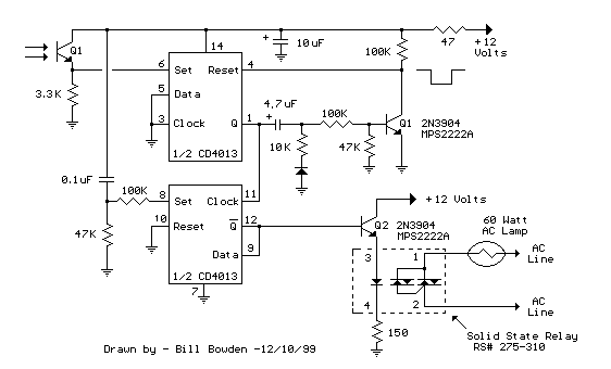
The IR photo transistor Q1 (Radio Shack 276-145A) or a similar component is connected to the set input (pin 6). It is essential to shield the photo transistor from direct light to ensure that the voltage at the set...
The intersection of industry and data collection systems includes hydrometeorological control systems, robot control systems, and digital image transmission systems. This is facilitated by the electron transport of data information. The data transmission system is a crucial component of...

Typically, home appliances are controlled using switches, sensors, and similar devices. However, physical contact with switches can pose risks, especially in the event of a short circuit. The circuit outlined here eliminates the need for physical contact to operate...
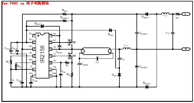
The IR2156 provides a cost-effective solution for fluorescent electronic ballasts. It integrates features such as lighting tube error protection and a programmable working frequency, which includes warm-up, lighting, and continuous operation of the ballast. The IR2156 is a highly integrated...
MSP430 microcontroller and I2C-compatible slave peripheral device. Temperature measurement tasks can be accomplished in a variety of ways. The MSP430 microcontroller is a low-power, 16-bit device widely used in embedded systems, particularly for applications requiring efficient power management and precise...