
Common base transistor amplifier circuit of a unit

The common base transistor amplifier is a configuration that offers unique advantages, particularly in high-frequency applications. The circuit operates with the transistor in a common base mode, where the base terminal is common to both the input and output signals. This configuration results in a low input impedance and a high output impedance, making it suitable for applications where impedance matching is critical.
In this circuit, the biasing resistors are crucial as they set the operating point of the transistor. The values of these resistors must be calculated to ensure that the transistor operates in the active region, preventing distortion of the amplified signal. The load resistor (Rc) at the collector plays a significant role in determining the voltage gain of the amplifier, while the AC coupling capacitors (C1 and C2) ensure that only the AC component of the signal is amplified, blocking any DC offset that could affect the performance.
Capacitor Cb is particularly important in this configuration, as it serves to decouple the base from ground, thus mitigating the effects of negative feedback that could otherwise limit the gain of the amplifier. By providing a stable DC operating point while allowing AC signals to pass, Cb enhances the amplifier's performance.
The input signal is applied to the emitter terminal, where it interacts with the base-emitter junction to control the flow of current from the collector to the emitter. The output signal is taken from the collector, which reflects the amplified version of the input signal. This arrangement allows for effective signal amplification with minimal distortion, making the common base amplifier a valuable choice in RF amplification and other high-frequency applications where signal integrity is paramount. Common base transistor amplifier circuit of a unit Common base amplifier basic structure of the circuit as shown, one of the key components primarily biasing resistor, capacito r coupling and amplifying transistor. Four resistors in the circuit to establish the quiescent point is provided, wherein the collector also possesses Rc (c) a load resistor functioning as; the load resistor RL is resistor; cl and C2 are two capacitors play a role through AC coupling DC blocking capacitor; decoupling electrical pit, Cb is to make the base (b) direct exchange ground, played the role of decoupling station, that is, from the elimination of the exchange of negative feedback effect. The input signal is loaded into the transistor emitter (e) and the base (b) between the output signal from the transistor collector (c) and between the base (b), shows that the base (b ) for the input signal and the output signal common terminal, therefore, the circuit is called a common base transistor amplifier.
Related Circuits
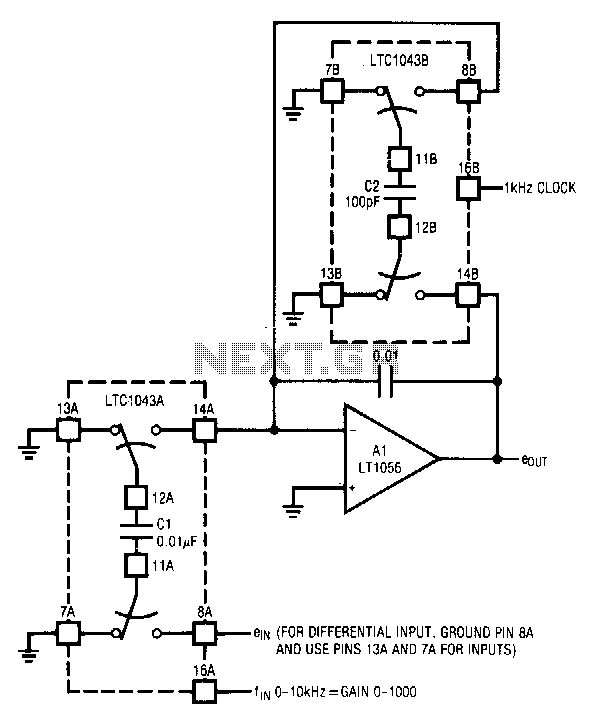
The circuit utilizes the LTC1043 in a variable gain amplifier configuration, which offers continuously adjustable gain, gain stability of 20 ppm/°C, and supports both single-ended and differential inputs. Two separate LTC1043 devices are employed in the design. The LTC1043B...

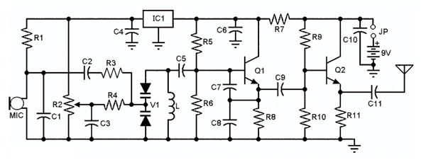
The sound mixer circuit is designed for service applications. This mixer is straightforward to implement and cost-effective, as it consists of two transistors along with a few simple resistors and capacitors. The sound mixer circuit typically utilizes two transistors configured...
Construct a low-power FM transmitter using surface-mount devices (SMD) that can be received by a standard FM radio. The proposed low-power FM transmitter circuit utilizes surface-mount devices (SMD) to achieve compactness and efficiency. The primary components of the circuit include...
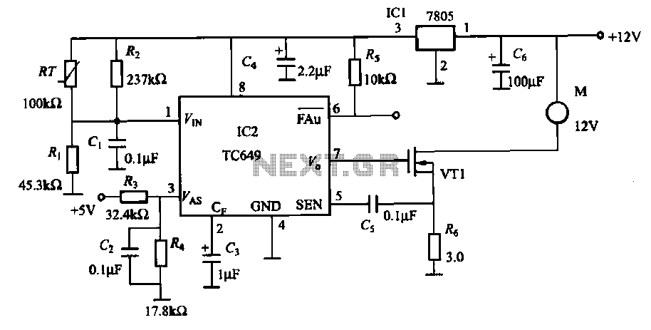
A motor is a heating device that can overheat, often due to accidents or overloads caused by excessive coil winding temperatures. The TC649 motor overheating protection and drive circuit, depicted in FIG. 1-9, utilizes an NTC thermistor (RT) positioned...
The schematic for the board is illustrated below. The three primary components of the board include (1) the power input and voltage regulation, (2) the L297 input and outputs, and (3) the L298 stepper motor control circuit. The motor...
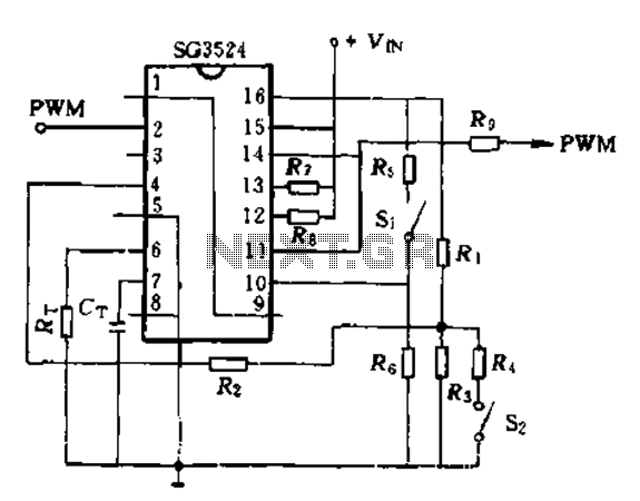
The SG3524 is utilized solely as a pulse width modulator. The error amplifier is configured in a follower arrangement. As illustrated in Figure 10-7, the ACR output connects to PWM output pin 2, which serves as the control signal....