
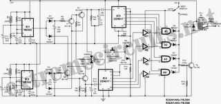
Crystal oscillator circuit consists of several gates as the d

The crystal oscillator circuit utilizes the piezoelectric properties of a quartz crystal to generate a stable frequency output. The fundamental operation involves the crystal acting as a frequency-selective element, which is integrated with active components such as operational amplifiers or logic gates to form an oscillator configuration.
In figure (A), the 1 MHz oscillator may employ a simple inverter or buffer configuration that provides the necessary feedback for oscillation. The crystal is connected in a feedback loop, ensuring that the oscillation frequency is determined by the crystal's resonant frequency.
Figure (B) illustrates a 20 MHz oscillator, which may utilize a similar topology but with adjusted component values to accommodate the higher frequency. The circuit design must ensure that the gain and phase conditions are met for sustained oscillation, often requiring careful selection of passive components such as resistors and capacitors.
The variable crystal oscillator circuit in figure (C) incorporates a mechanism, such as a variable capacitor or an adjustable inductor, allowing the oscillation frequency to be tuned within the specified range of 2-20 MHz. This adaptability is crucial for applications requiring frequency modulation or precise frequency adjustments.
Figure (D) depicts a variable oscillator circuit operating between 5-10 MHz, which may utilize a combination of fixed and variable components to achieve the desired frequency range. The design should maintain stability across the variable frequency range to prevent unwanted frequency drift.
Finally, figure (E) presents a dual-loop crystal oscillator circuit. This configuration typically enhances frequency stability and reduces phase noise by employing two feedback paths. One loop may provide coarse frequency control, while the other offers fine-tuning, achieving superior performance in precision applications.
Overall, crystal oscillator circuits are fundamental in various electronic devices, providing reliable timing references essential for synchronization in communication systems, microcontrollers, and other digital applications. The design intricacies of each oscillator type highlight the importance of component selection and circuit topology in achieving desired performance characteristics.Crystal oscillator circuit consists of several gates as the d Several gates as shown by a crystal oscillator circuit. FIG. (A) to l MHz crystal oscillator circuit, the figure ( b) is 20 MHz crystal oscillator circuit, hide in (c) is variable 2-20 MHz crystal oscillator circuit, FIG. (D) is 5 --10 MHZ variable oscillator circuit diagram (e) of the dual-loop crystal oscillator circuit.
Related Circuits
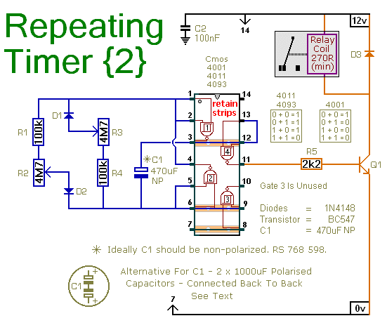
This circuit is based on a simple asymmetric oscillator. The duration for which the relay remains energized and the duration for which it remains de-energized are independently set. With the component values indicated in the diagram, both durations are...
When this circuit is connected to a filter and an oscilloscope, the oscilloscope displays the filter's frequency response. A frequency that sweeps from low to high is applied to a filter. The oscilloscope is triggered by the start of...
An astable multivibrator is a switching circuit that alternates its output on and off for a designated time period. This device, also known as a free-running oscillator circuit, is primarily utilized to generate square waves over a specified duration....
Q1 and Q2 form a constant current drive defined by R2. The current (I) approximates the reciprocal of R2 in the circuit shown for values of I greater than 1 amp. The pulse current is drawn from C1, which...
The following circuit illustrates an Automatic Room Power Control Circuit Diagram. This circuit is based on the NE555 integrated circuit (IC). Features include the use of two Light Dependent Resistors (LDRs). The Automatic Room Power Control Circuit utilizes an NE555...
Trimming is straightforward when matched NPN transistors are utilized for Q1 and Q2, along with 1% tolerance resistors for R6 to R11. A dual trace oscilloscope, digital voltmeter (DVM), and sine wave generator are required for this process. Although...