
Cutting good performance signal switching circuit

The circuit involves the use of analog switches SL and SA, which are crucial for controlling the flow of signals based on the logic state. When the inverted logic signal is applied to terminal 2, it activates switches S1 and S4, creating a path for capacitance coupling between S1 and S8. This configuration is essential for ensuring that the signals can interact without direct electrical connection, thereby maintaining isolation while allowing for signal transmission.
The on-state resistance of the switches, which is specified to be between 50 and 100 ohms, plays a significant role in determining the overall signal integrity and performance of the circuit. Lower on-state resistance typically results in reduced power loss and improved signal fidelity.
Additionally, the operational buffer amplifier serves to isolate the input from the output, providing a high input impedance and low output impedance. This characteristic is vital for preventing loading effects on the previous stage of the circuit. The choice of resistor R2 should be made considering the availability of components and the desired voltage gain, which is specified as 4.1 +/- 1. This gain setting can be critical for applications requiring specific signal levels, ensuring that the output remains within acceptable limits for further processing or interfacing with other circuit stages.
Overall, the described circuit configuration is designed to facilitate efficient signal management while maintaining the necessary performance characteristics through careful selection of components and design parameters.Analog switches sl and sa disconnect, Ctz the inverted logic signal to terminal 2 s! And 84 is turned on, so that prisoners capacitance between S1 and S 8 and coupling will be generated and S 2 and 8 4 shunt (on-state resistance 50 ~ lOOQ). OP buffer amplifier is a buffer amplifier. Rz need to choose according to the availability of several scrimp 4 1 +/l where the voltage gain.
Related Circuits
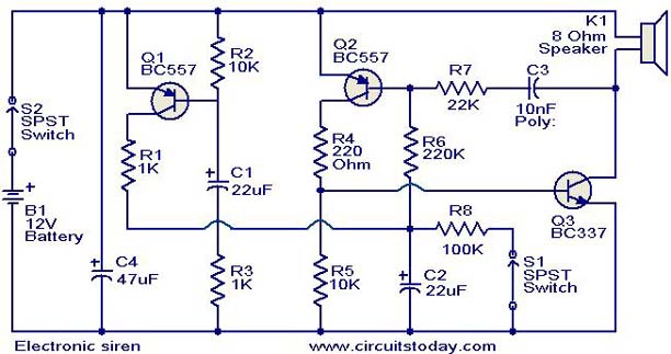
This is a compact electronic siren circuit based on three transistors. This circuit is suitable for incorporation with other alarm or siren projects such as burglar alarms, automatic factory sirens, or a simple push-to-on alarm. The electronic siren circuit...
The circuit operates as follows: each morning, light enters the silicon photocell, generating a force that causes transistor VT1 to conduct. As a result, capacitor C charges, leading to an increase in voltage. This rising voltage causes the emitter...
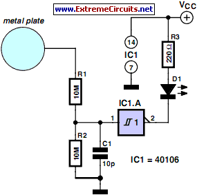
This simple circuit can be utilized to activate various devices, such as microcontrollers, relays, secret alarms, or robot applications. It can also be used to turn on LED1, which remains illuminated as long as the metal plate is touched....
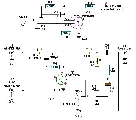
A simple and efficient active antenna electronic project can be designed using this electronic schematic circuit based on transistors. This active antenna project is effective for a wide range of RF frequencies, covering three RF bands: HF, VHF, and...
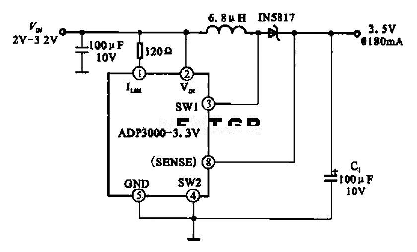
Boost 3.5V regulator circuit. This chip can boost or create a stable voltage supply from approximately 3V DC to a DC voltage of 3.5V. The boost regulator circuit is designed to increase a lower DC voltage, specifically from around 3V...

The circuit produces a pleasing and accurate imitation of sound, making it suitable for sound effects such as doorbells. It generates a two-tone effect that closely resembles the sound of a cuckoo. This circuit is designed to create a two-tone...