
CV/CC charger circuit diagram designed using LinKSwitch

The described circuit is a compact and efficient solution for low-power charging applications. The LinKSwitch family IC serves as the core component, effectively managing the power conversion process while ensuring that the output remains stable under varying load conditions. The design utilizes a full-wave rectifier configuration with diodes D1 through D4, which converts the incoming AC voltage to a pulsating DC voltage. This rectified voltage is then smoothed out by the bulk capacitors C1 and C2, which serve to minimize voltage ripples and provide a stable DC output.
The inclusion of inductor L1 in conjunction with capacitors C1 and C2 forms a pi filter that is critical for reducing electromagnetic interference (EMI). This feature is particularly important in applications where sensitive electronic devices are present, as it helps to maintain compliance with EMI regulations and ensures reliable operation without interference.
The LinkSwitch-II IC, designated as U1 in the schematic, is a highly integrated solution that simplifies the design process. It combines several essential functions, including power switching, oscillation, and control, into a single package. This integration not only reduces the overall component count but also enhances the reliability of the circuit. The built-in 700V MOSFET provides adequate voltage headroom, allowing the charger to operate effectively across a wide range of input voltages, making it suitable for global applications.
Overall, this 3.25W CV/CC charger design exemplifies an efficient and reliable approach to power management, leveraging advanced semiconductor technology to deliver a stable output while minimizing size and complexity.A very simple 3. 25W CV/CC charger can be designed using LinKSwitch | family IC manufactured by Power Integrations. This electronic circuit project is designed to provide a 5 volts output at a maximum current of 650mA. This 3. 25W CV/CC charger, needs to be powered using a AC voltage between 85 and 265 VAC. The AC input power is rectified by dio des D1 through D4. Bulk storage capacitors C1 and C2 filter the rectified AC. Inductor L1 forms a pi ( ) filter with C1 and C2 to attenuate conducted differential-mode EMI noise. The LinkSwitch-II device (U1) incorporates the power switching device, an oscillator, a CC/CV control engine, startup circuitry, and protection functions into one IC. The integrated 700 V MOSFET allows sufficient voltage margin for universal input AC applications. 🔗 External reference
Related Circuits

The transmitter is constructed on a Printed Circuit Board (PCB). This board incorporates track inductors for L1, L2, and part of L3. The section surrounding Q1 functions as the oscillator section, with the oscillation frequency determined by L1, C4,...
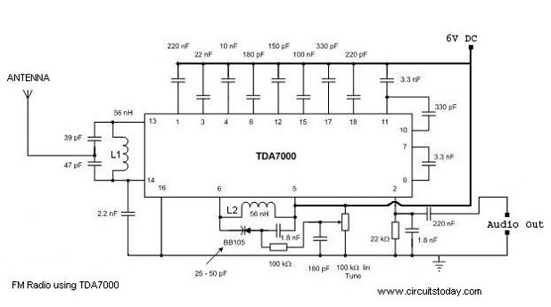
A simple FM radio circuit with a diagram and schematic using the IC TDA 7000. This low-cost single-chip FM radio circuit design is easy to assemble and is suitable for creating a portable FM radio. The FM radio circuit utilizing...
These small electronic lamps are quite practical and have a long lifespan. Approximately 40 years after Nick Holonyak invented the first LED, they have become nearly essential. Any dedicated electronics enthusiast typically keeps a few in their collection. Prior...
The Accu charger circuit is straightforward and simple to construct, requiring no more than ten components. In addition to its ease of assembly, this charger circuit is also cost-effective and highly efficient. The circuit requires a power supply from...
This circuit is representative of the typical application of a photomultiplier tube. The circuit depicted is AC coupled; however, if DC coupling is required, the capacitor can be removed, and an appropriate interfacing method should be employed. A common...
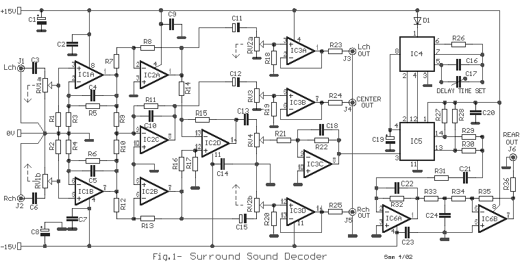
The circuit operation begins by transmitting stereo surround sound signal quality information through the master volume circuit. This drives the left channel connected to the LCH Model TL072 IC1A and IC1B, which are linked to the right channel (Rch)....