
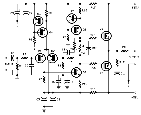
DC-coupled multi-stage amplifier circuit b

The DC-coupled multi-stage amplifier circuit is designed to provide high gain while maintaining linearity across the amplification stages. Each stage is carefully biased to ensure that the transistors operate in their active regions, thus allowing for efficient signal amplification. The use of NPN transistors in the initial stages capitalizes on their high current gain characteristics, while the inclusion of PNP transistors helps to stabilize the output voltage by counteracting the rising DC levels that can occur through cascading stages.
In this configuration, the collector of each NPN transistor connects to the base of the subsequent transistor, creating a chain of amplification. The base biasing resistors are selected to set the appropriate quiescent operating points, ensuring that each transistor remains within its linear operating range. The progressive increase in collector potential is managed by the strategic placement of PNP transistors, which serve to pull down the voltage levels as needed, thereby preventing saturation and distortion in the output signal.
The emitter follower configuration is particularly useful in this design as it provides a low output impedance, which is advantageous for driving loads. This stage can effectively isolate the previous amplification stages from the load, allowing for improved signal integrity and reduced loading effects. By using diodes in conjunction with the emitter follower, the circuit can further clamp the DC levels, ensuring that the output remains stable across varying input conditions.
Overall, this DC-coupled multi-stage amplifier circuit exemplifies a robust design approach for achieving high fidelity amplification in various electronic applications, from audio processing to signal conditioning in instrumentation. Proper component selection and biasing are critical to the performance of the circuit, ensuring that it meets the desired specifications while minimizing distortion and maintaining a wide dynamic range.DC-coupled multi-stage amplifier circuit b (3) multi-stage DC-coupled amplifier in DC-coupled by a multi-stage amplifier circuit amplifying circuit, if used NPN type transistor of each stage, in order to fit all levels have appropriate operating point of stage base, Step by step the collector potential increases, so reducing the final output voltage range. In order to solve this problem, in practice, it can be used in conjunction with NPN and PNP transistor to reduce the post-stage DC potential, as shown in FIG.
Figure (8) shows an NPN cvri) _ and PNP transistor (VT2) wish, is used to reduce the subsequent stage (VT3) potential. Alternatively, you can use emitter follower, stage amplified voltage diode to reduce a DC potential of the circuit.
Figure (b) shows the use of emitter cvn) is used to reduce the subsequent stage (, rr3) potential.
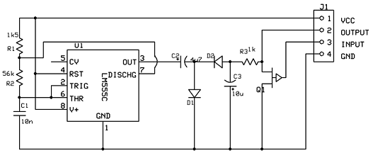
Related Circuits
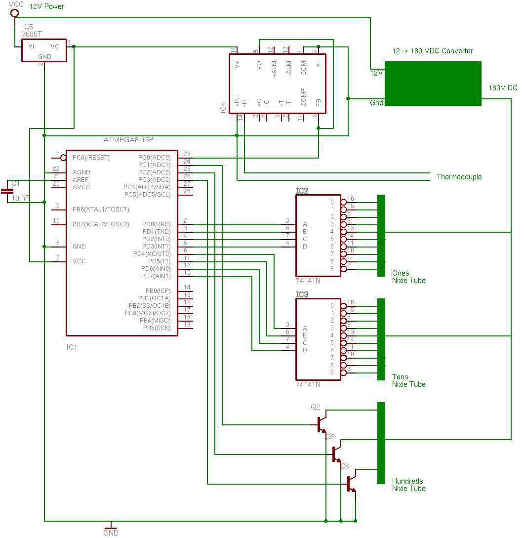
the entire circuit is comprised of integrated circuits. This makes for some easy organization when it goes to the circuit board for soldering. In addition, I used only 3 of the pins on the 3rd nixie tube for the...

This simple water level sensor circuit monitors the presence of water in a specific location or container. The circuit activates an acoustic alarm when it detects water. The water level sensor circuit typically consists of several key components, including a...
The input capacitor is used for low-frequency cut-off, with a standard value of 0.1 µF, resulting in a cut-off frequency of approximately 16 Hz. The input capacitor plays a crucial role in filtering unwanted low-frequency signals in electronic circuits. By...
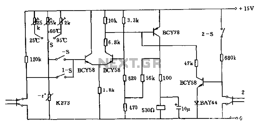
The circuit utilizes a thermistor (K273) to monitor temperature levels and control a relay based on the immersion of two sensor electrodes in a liquid. When the temperature reaches a predetermined threshold, the relay activates to heat the liquid....
Can be directly connected to CD players, tuners and tape recorders. Simply add a 10K Log potentiometer (dual gang for stereo) and a switch to cope with the various sources you need. A correct grounding is very important to...
Our programmable MP3 player has an interface to an LCD with a HD44780 controller. These are alphanumeric LCDs with one to 4 lines of text and 16 to 40 characters per line. However, these LCDs (and LCDs in general)...