
DC-DC Convertor

This circuit operates as a simple DC voltage regulator using a zener diode to maintain a stable output voltage. The primary components of the circuit include a zener diode, a resistor, and a load. The input voltage is supplied from a 12V battery, which is higher than the desired output voltage of 9V.
The zener diode is selected based on the required output voltage; in this case, a 10V zener diode is used. When the input voltage exceeds the zener breakdown voltage, the diode conducts and clamps the output voltage to approximately 9.3V under a load current of 100mA. The resistor, connected in series with the input voltage, limits the current flowing through the zener diode and ensures safe operation. The value of the resistor must be calculated based on the input voltage, output voltage, and the expected load current to ensure that the zener diode operates within its specified limits.
The output voltage can be adjusted by selecting different zener diodes with varying breakdown voltages, allowing for flexibility in applications requiring different DC output levels. The circuit's performance can be influenced by variations in the input voltage, which can be analyzed through the provided graph, illustrating the relationship between the input voltage and the output voltage under specific load conditions. This simple yet effective design is widely used in various electronic applications where a stable and lower voltage is required from a higher voltage source.This circuit will generate a smaller DC output voltage from a larger DC input voltage.It is quick and simple to make and by changing the value of the zener diode, the circuit can be universally adapted to provide other output voltages.The circuit and all diagrams represent a DC convertor with 12V battery input and 9Volt DC output. With the 10V zener diode as shown in the diagram the output voltage is about 9.3 Volts DC. The above graph shows how the output is affected by input voltage variations. This was produced with a load current of 100mA and using a 10 volt rated zener diode. 🔗 External reference
Related Circuits
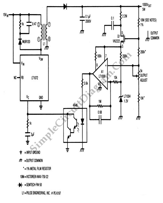
The circuit illustrated in the schematic diagram below is an isolated DC-to-DC step-up converter. The term "isolated" indicates that there is no electrical connection between the input and output sections of the circuit. The isolated DC-to-DC step-up converter operates by...
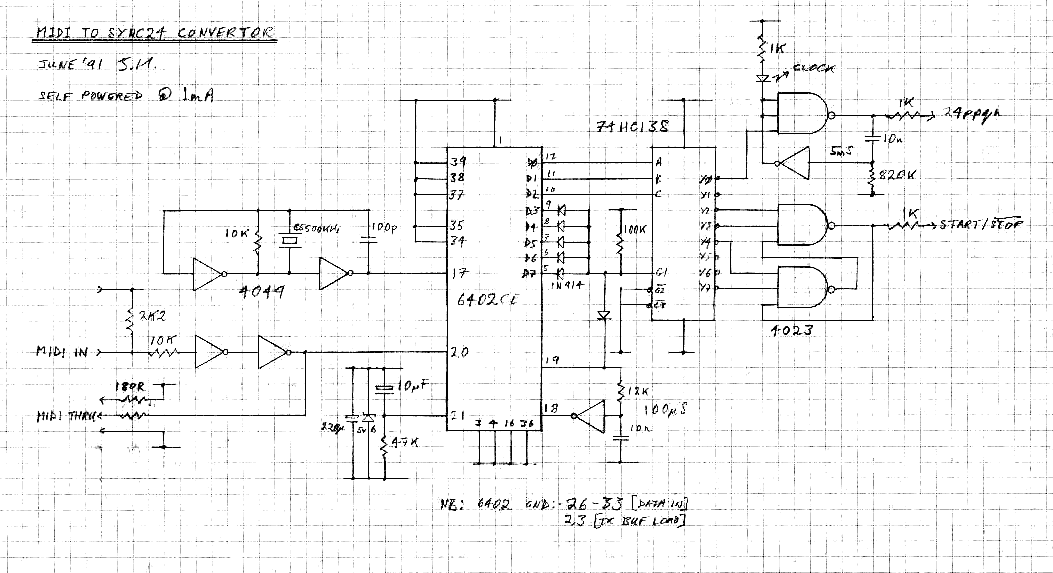
This self-powered circuit converts MIDI clocks to DIN sync24. This type of clock is used on old Roland gear and provides a 24 pulses per quarter note clock and a start/stop signal. The circuit functions by receiving MIDI clock signals,...
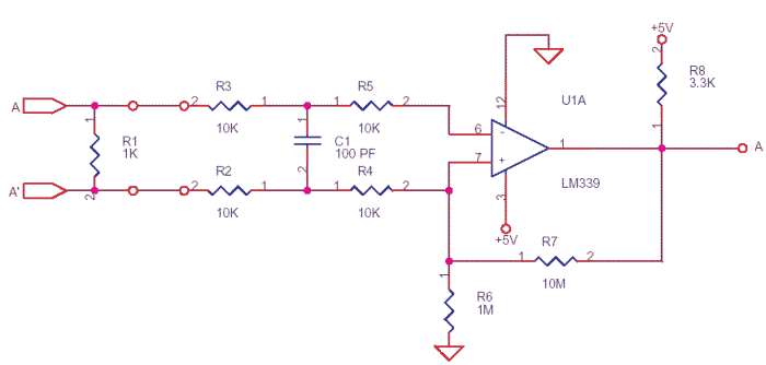
The differential outputs are balanced and designed to drive long lengths of coaxial cable, stripline, or twisted pair transmission lines with characteristic impedances ranging from 50 ohms to 500 ohms. Differential transmission is superior to single-wire transmission as it...
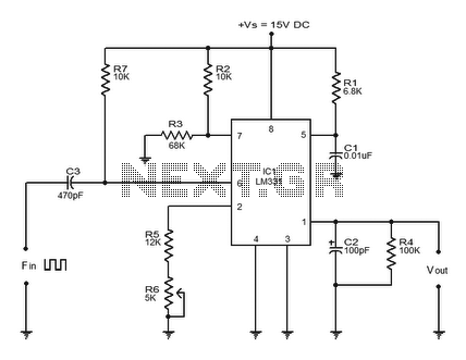
Converter circuits are commonly utilized in various applications, and there are several types available. A simple frequency-to-voltage converter circuit uses the IC LM331, which is essentially a precision voltage-to-frequency converter. This IC has numerous applications, and in this instance,...
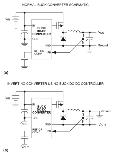
Any step-down DC-DC converter can be utilized as an inverter without modifications to the operating schematic. The only differences between the standard step-down application and the inverting operation are the labels of the connection points. The step-down VOUT is... A...
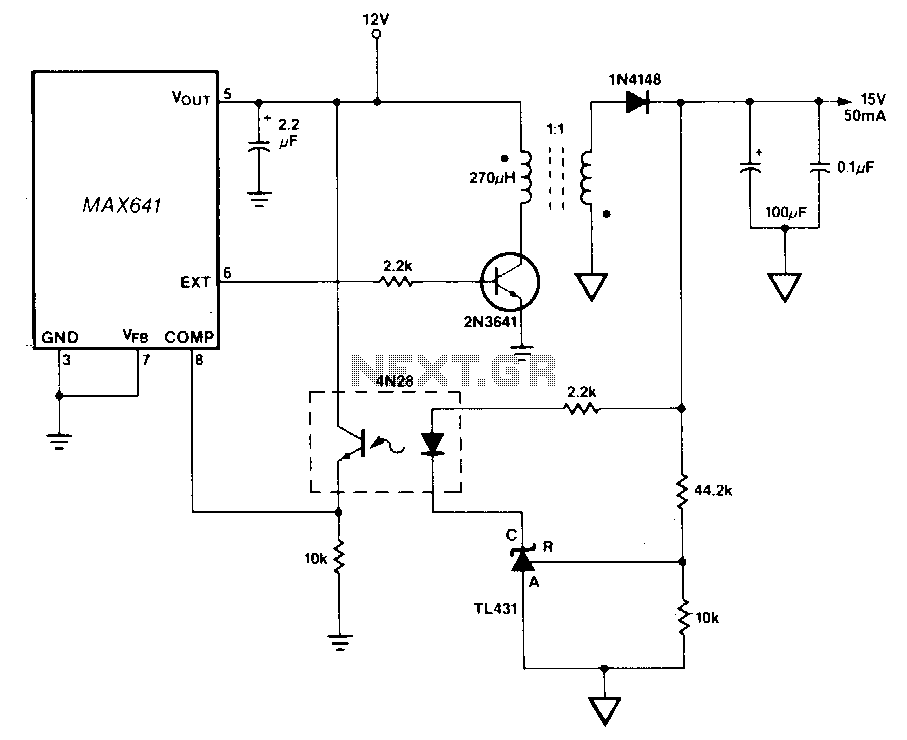
In this circuit, a TU31 shunt regulator is utilized to monitor the output voltage. The TU31 activates the LED of a 4N28 optocoupler, which delivers feedback to the MAX641 while ensuring isolation between the input voltage of +12 V...