
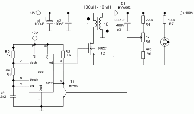
dc to dc converter

The described DC to DC converter circuit operates by employing a center-tapped transformer, which is a critical component in this design. The transformer is energized by a blocking oscillator, a circuit configuration that allows for the conversion of direct current (DC) into alternating current (AC) and subsequently back into a higher DC voltage. The blocking oscillator works by rapidly switching the current flow, causing the transformer to generate an alternating voltage on its secondary winding.
The center-tapped transformer provides two equal voltage outputs from its secondary winding, which facilitates the generation of a high voltage by utilizing half of the winding. The output voltage is further amplified through a voltage tripler circuit. This voltage tripler consists of three capacitors and three diodes arranged in a specific configuration that allows the circuit to effectively multiply the voltage output from the transformer.
During operation, the first diode conducts during the positive half-cycle of the AC voltage from the transformer, charging the first capacitor. In the subsequent half-cycle, the second diode conducts, allowing the second capacitor to charge while the first capacitor retains its charge. The third diode then allows for the combination of the charges from the first two capacitors, effectively tripling the input voltage. The final output voltage is available for low power applications, making this circuit suitable for devices that require a high voltage supply but do not demand high current.
It is important to note that while this circuit is capable of producing high voltages, its overall efficiency is limited. Factors contributing to this inefficiency include losses in the transformer, voltage drops across the diodes, and the inherent capacitance and leakage currents in the capacitors. Despite these limitations, the circuit remains a viable solution for applications where high voltage is necessary, but where efficiency is not the primary concern. Proper design considerations, such as selecting appropriate component ratings and ensuring adequate heat dissipation, are essential for reliable operation.The circuit is a DC to DC converter using a standard 12 VAC center tapped power transformer wired as a blocking oscillator. The circuit is not very efficient but will produce a high voltage usable for low power applications. The input battery voltage is raised by a factor of 10 across the transformer and further raised by a voltage tripler consisting of three capacitors and diodes connected to the high voltage side of the transformer..
🔗 External reference
Related Circuits
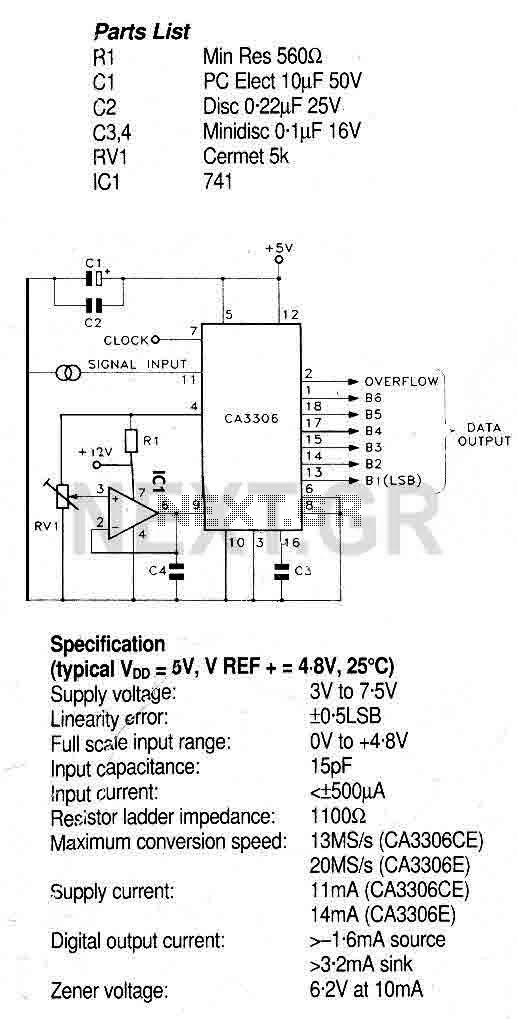
This circuit utilizes the CA3306, a family of CMOS parallel (flash) analog-to-digital converters designed for low power and high-speed applications. The CA3306CE operates at sampling rates of up to 10 million samples per second, while the CA3306E can achieve...
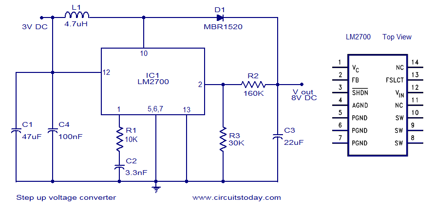
A simple DC to DC step-up voltage converter circuit schematic using the LM2700, which is a step-up switching converter. The LM2700 is a versatile step-up switching converter designed to efficiently convert a lower input voltage to a higher output voltage....
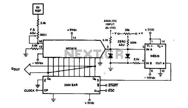
The time IO-bit conversion operates at 3.3 MHz with a clock signal. This converter utilizes a 2504 12-bit register in successive approximation mode, where the conversion signal for the short-cycle end is derived from the first bit utilized in...
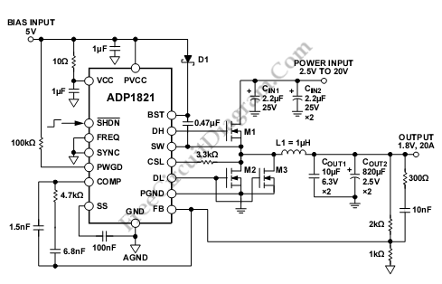
This is an ADP1821 step-down DC-to-DC converter circuit. This circuit utilizes the ADP1821, which is a synchronous pulse-width-modulated (PWM) step-down controller. The ADP1821 is designed to efficiently convert a higher input voltage to a lower output voltage while maintaining high...
This circuit utilizes the NE555 integrated circuit configured as a stable multivibrator. It generates a rectangular wave frequency of approximately 100 Hz, outputting from pin 3 through capacitors C3 and C4, preceding the rectifier power section. The circuit employs...
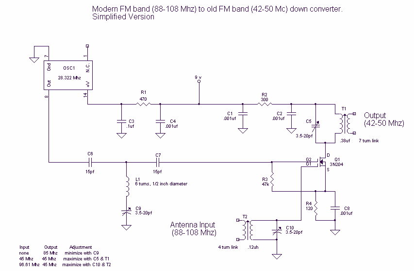
Before World War II the FM radio band was just below 50 Mc. Read all about it. If you have such a radio, you might want to build this converter. It will let your old set receive the modern...