
DC to DC converter electronic schematic

The described circuit utilizes the TLC555 or 7555 timer IC in an astable configuration to generate a square wave signal. This signal oscillates at approximately 20 kHz, which is suitable for the intended application of voltage conversion. The frequency is determined by the resistors A2 and A3 and capacitor C1, which set the timing characteristics of the oscillator.
The generated square wave is then directed to a voltage doubler rectifier circuit. This circuit consists of two Schottky diodes (O1 and O2) and capacitors C3 and C4. Schottky diodes are preferred due to their lower forward voltage drop, which enhances efficiency in voltage conversion. The use of capacitors C3 and C4 is critical; C3 charges to the peak voltage of the waveform, while C4 serves to smooth the output voltage, providing a stable -9 V output.
Capacitor C5 acts as a high-frequency noise filter, ensuring that the output voltage is clean and stable. The role of A1, along with capacitors C6 and C7, is to manage the power supply to the timer, preventing unnecessary power draw when the circuit is not in use.
The overall design emphasizes efficiency and compactness, making it suitable for integration into various electronic devices. The PCB layout should consider the proximity of components to minimize parasitic inductance and capacitance, which could affect performance. The circuit is designed to maintain a stable output voltage under a maximum load current of 10 mA, making it suitable for low-power applications requiring a negative voltage.Those of you who frequently use devices that work on battery or you need a negative trend at the moment you have a single positive, will definitely look for a converter like the one described below. Constructing it, you can convert a positive voltage of a battery of 9 V to negative using well known integrated 555.
The same circuit can also be used in cases those requiring two symmetrical lines of power, when available a single battery. The integrated TLC555 is the old bipolar NE555, manufactured with technology but CMOS. Unless you have this type of integrated, you might as well use an 7555. In this construction, the TLC555 is syndesmologimeno arranged in a ground unstable. The oscillation frequency determined by the A2, A3, C 1 and approaching 20 kHz. The rectangular waveform produced by the oscillator is therefore time to time (Duty Cycle) close to 50%. The waveform is led to a rectifier Doubler formed by C3, O1, O2 and C4. In place of O1 and O2 should be placed diodes Schottky type VAT85 due to low voltage correct direction which is equal to 0,4 V (silicon diodes such as type 1 N4148, show a tendency equal to 0,7 V).
The capacitor C4 cares for smoothing the voltage bristled, while the C5 relieve the signal from noise high frequencies. With the help of A1, C6 and C7 achieved the disconnection of supply voltage timer. The consumption of the inverter to power depends largely on the load to be connected to the output of -9 V.
As seen from the values ??indicated in the table, the output voltage is held within tolerable levels, as the load current is kept less than 1O mA. To make it easy to integrate the inverter into any electronic device, I suggest you build a small PCB board.
Related Circuits

When the water level is below the steel rods, there is no contact between the metal can and the rods, which are supported by a small insulated wooden board. The circuit built around IC1 draws no current, resulting in...
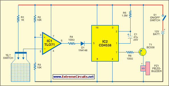
Protect your valuable laptop against theft using this miniature alarm generator. Fixed inside the laptop case, it will sound a loud alarm when someone tries to take the laptop. This highly sensitive circuit uses a homemade tilt switch to...
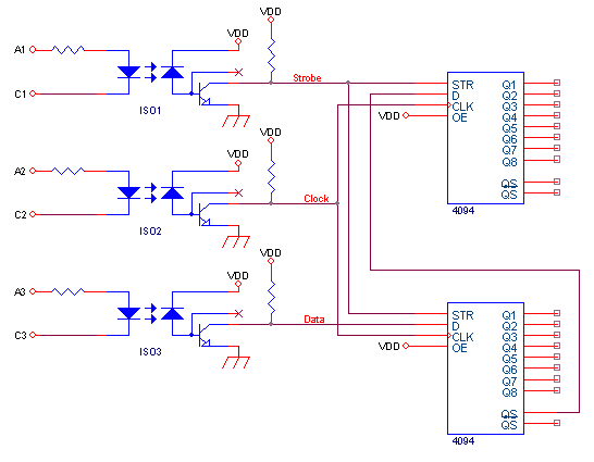
This circuit connects to a single parallel port, enabling control of electronic circuits that require up to 96 digital outputs with optically isolated lines, powered by 3 to 15V. The CD4094B is an 8-bit shift register combined with an...
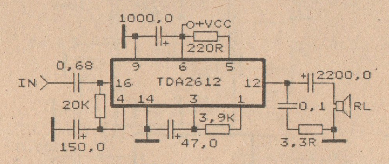
This amplifier circuit is based on the IC TDA2612 produced by Siemens. The minimum voltage required for this circuit is 10 volts, while the maximum voltage is 35 volts DC. The power output is 25 watts with a 4-ohm...
The series consists of input buffers that match the output. This configuration resembles a common collector circuit with a reinforcement factor of 1. A resistor value is included to limit the current usage. The effectiveness of this circuit largely...
L2 RFC (resistance 1MOhm with an inductor wrapped around it, composed of multiple coils made from fine insulated wire. The scratch of the inductor connects to the resistance, forming a parallel L-R circuit.) With capacitors C7 and C8, we...