
DDR memory power supply circuit
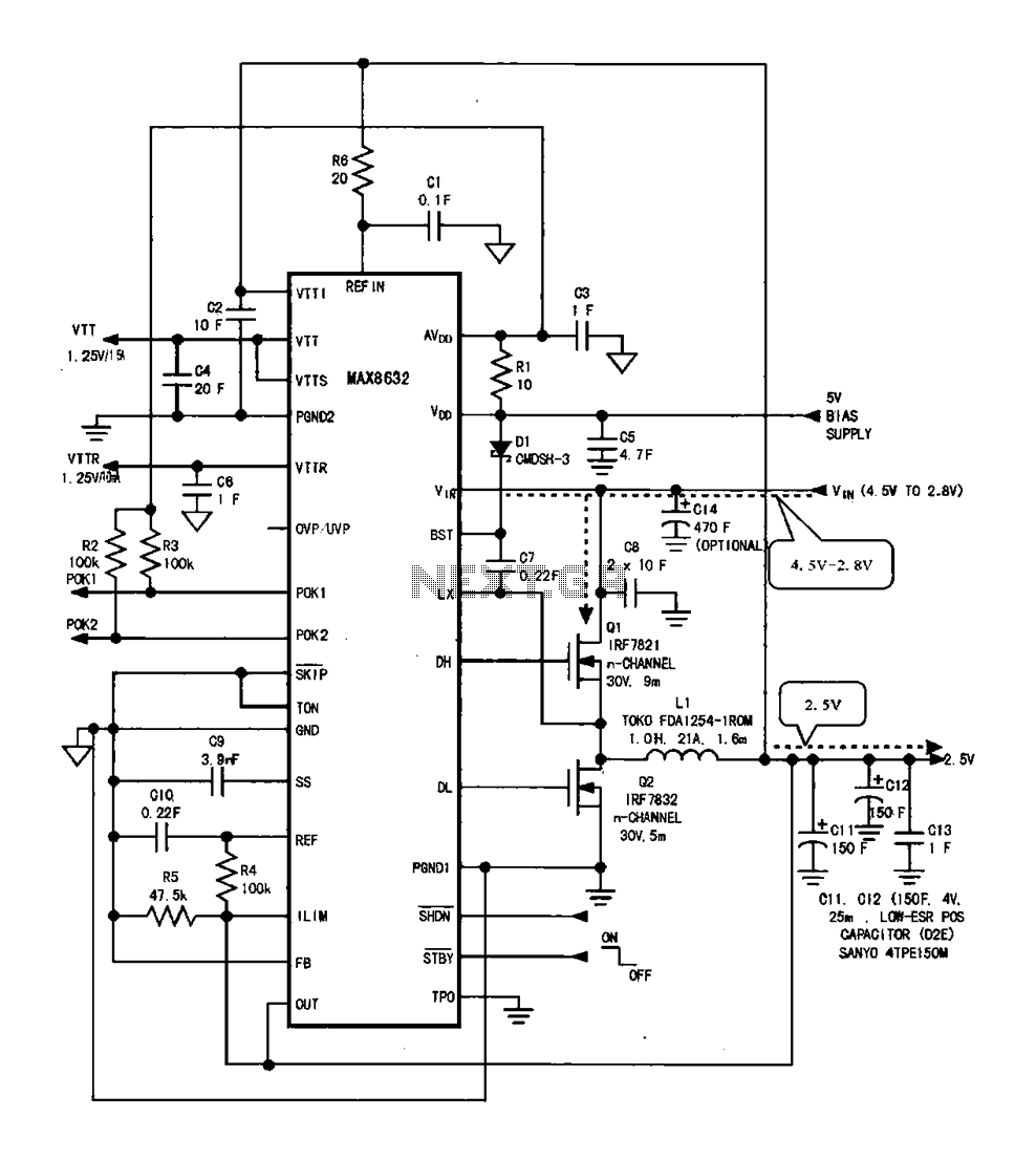
The DDR memory power supply circuit is designed to efficiently convert a variable DC battery voltage into a stable output voltage suitable for DDR memory operation. The MAX8632 chip serves as the core component of the power control circuit, managing the power supply by generating pulse-width modulation (PWM) signals. These PWM signals are crucial for controlling the switching action of the field effect transistors Q1 and Q2, which are configured in a push-pull arrangement.
The operation begins with the detection of the battery voltage, which can range from 4.5 V to 2.8 V. This range is essential for ensuring compatibility with various battery types and states of charge. The MAX8632 monitors this voltage and adjusts the PWM signals accordingly to maintain the desired output voltage. The switching voltage applied to the drain of Q1 allows for the modulation of the input battery voltage.
Transistors Q1 and Q2 are key components in this circuit, as they alternately conduct based on the PWM signals they receive. When Q1 is turned on, it allows current to flow from the battery through the load, while Q2 is turned off, and vice versa. This complementary operation ensures that the output voltage remains stable despite variations in the input voltage or load conditions.
The LC filter, composed of an inductor (L) and a capacitor (C), smooths the PWM output to produce a consistent 2.5 V output. This filtered voltage is crucial for the reliable operation of DDR memory, which requires a stable power supply to function correctly. The design of the LC filter is critical, as it must effectively reduce ripple voltage while maintaining efficiency.
Overall, this DDR memory power supply circuit exemplifies a robust design that efficiently converts battery voltage to a suitable level for memory applications, ensuring reliable performance in notebook devices.DDR memory power supply circuit Shows the notebook DDR memory power supply circuit, the power control circuit chip MAX8632, the chip power supply terminal VDD is Sv (detection point 1), the battery DC supply voltage between 4.5 V-2.8 V, the the switching voltage is applied to the field effect transistor Ql drain power supply control chip DH, DL outputs a PWM pulse of opposite phase signals, which signals are applied to Ql, Q2 of the gate, under the action of the PWM pulse Q1, Q2 alternately working, the DC voltage of the battery becomes switching voltage, and then after the LC filter output voltage of 2.V for the memory circuitry.
Related Circuits
It is essential to draw a circuit using a layout and conventions that are universally recognized. In electronic circuit design, adherence to standardized symbols and layout conventions is crucial for effective communication among engineers and technicians. A well-drawn schematic diagram...
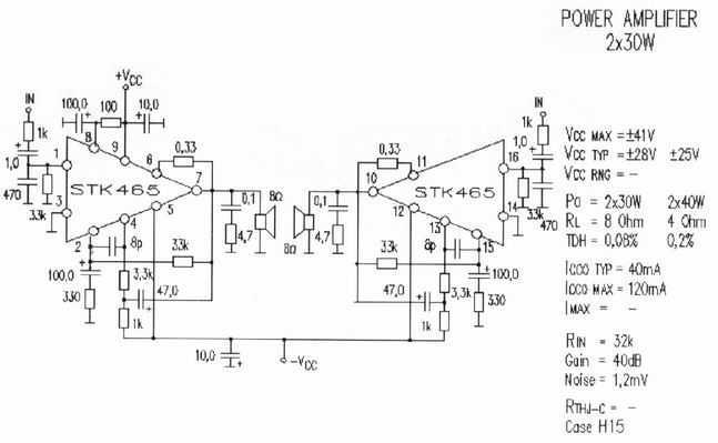
Completed STK465 is an amplifier of acoustic frequencies that offers qualitative output, using minimal exterior elements. Substantially he is one of big completed force. Has a line pins and incorporated metal surface for adaptation in cooler. The provision pins...
The transistors create a differential pair with an active current-source tail. This configuration, referred to as a variable-transconductance multiplier, produces an output that is proportional to the product of the two input signals. The multiplication effect arises from the...
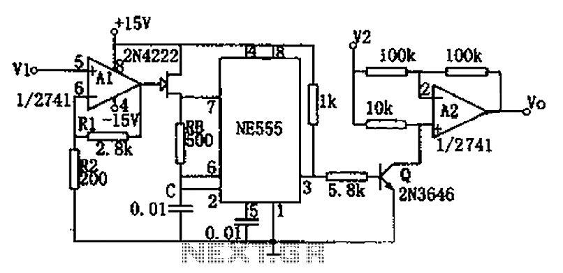
The circuit depicted in the figure consists of a voltage-frequency converter and an amplitude modulator. The input voltage V1, processed by operational amplifier A1, controls the FET 2N4222's internal resistance, which in turn alters the oscillation frequency of the...
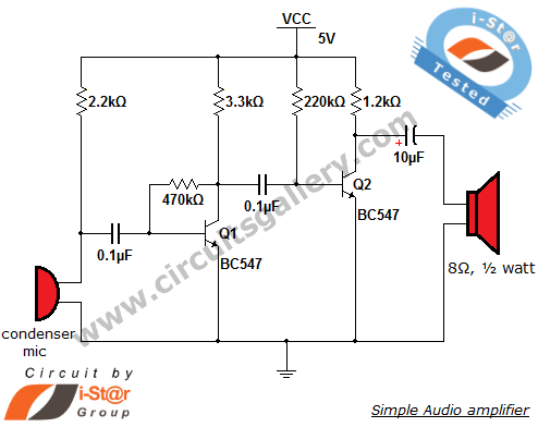
The output of the condenser microphone is coupled through a 0.1 µF coupling capacitor, which serves to eliminate DC components from the audio signal. Transistor Q1 is configured in a collector-to-base biasing mode, achieved with a 470kΩ resistor. This...

This is an Overheat Detector Alarm Switch using the Temperature Sensor IC LM35. The core of this overheat detector (fire alarm) circuit is a precision integrated temperature sensor, the LM35 (IC1), which provides an accurately linear and directly proportional...
Warning: include(partials/cookie-banner.php): Failed to open stream: Permission denied in /var/www/html/nextgr/view-circuit.php on line 713
Warning: include(): Failed opening 'partials/cookie-banner.php' for inclusion (include_path='.:/usr/share/php') in /var/www/html/nextgr/view-circuit.php on line 713