
NE555 circuit diagram of a divider circuit

The circuit integrates a voltage-to-frequency conversion mechanism with an amplitude modulation capability, facilitating the transformation of an input voltage signal into a frequency-modulated output. The operational amplifier A1 serves a crucial role in regulating the internal resistance of the FET 2N4222, which is essential for adjusting the frequency of the astable multivibrator. This configuration allows for precise control over the oscillation frequency based on the input voltage V1.
Operational amplifier A2 is tasked with amplitude modulation, where it processes the input signal V2 to produce a modulated output. The modulation depth and characteristics can be fine-tuned by adjusting the circuit components, particularly R1 and R2, which influence the pinch-off voltage of the FET. The relationship defined by Vo - V2/V1 indicates that the output voltage Vo is directly influenced by the ratio of the input voltages, emphasizing the need for careful calibration within the specified range of 0 to 10V.
To obtain the average output voltage Vo, a filtering stage is included, which smooths out the variations in the modulated signal. This filtered output can then be accurately measured using a damped voltmeter, providing a reliable means of monitoring the circuit's performance. The design demonstrates versatility and applicability in various electronic applications, particularly in signal processing where frequency and amplitude modulation are required. As shown in FIG circuit by the voltage - frequency converter and an amplitude modulator. Input voltage V1 by the operational amplifier A1 control FET 2N4222 internal resistance , thereby changing the astable multivibrator oscillation frequency. A2 is the amplitude modulator, modulated by the input signal V2 output. Let FET pinch-off voltage Vp,Tt (1 + R1/R2) Vp, the output and input of the relationship: Vo -V2/V1 V1 and V2 required range is 0 ~ 10V. Vo is the average output can be obtained through the filter, you can also use damped voltmeter readout.
Related Circuits
This circuit functions to monitor the duration of occupancy in a toilet, activating an alert if the time spent exceeds a predefined limit. The components involved include a resistor, integrated circuit (IC), capacitor, and transistor. The occupancy monitoring circuit is...

The electronic circuit simulates bird sounds under varying lighting conditions, particularly influenced by neon light irradiation, resulting in fluctuating and changing tones. The sound produced is continuously variable. The schematic of this circuit is provided. The described electronic circuit utilizes...

A series of LEDs that turn on and off in a precise sequence, creating a calming and hypnotic effect. Various LED chaser, scanner, and sequencer circuits exist, utilizing discrete transistors, logic integrated circuits (ICs), or microcontrollers. However, a common...
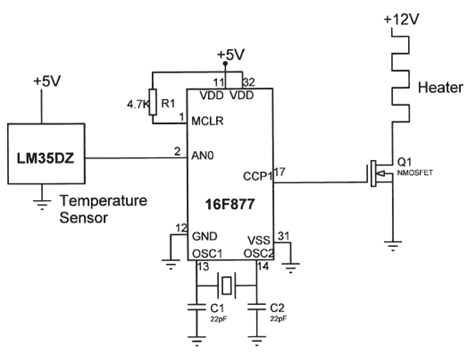
The electrical circuit diagram of this temperature control circuit consists of a 3-pin analog temperature sensor (LM35DZ), a built-in A/D converter microcontroller (PIC16F877), and the heater driver (IRL1004). The temperature control circuit utilizes the LM35DZ, a precision analog temperature sensor...

The PGA202 offset voltage correction circuit is designed to correct both input and output offset voltages. There are four different gain settings for the PGA202, which result in slight variations in input offset voltage. A 50k potentiometer is used...
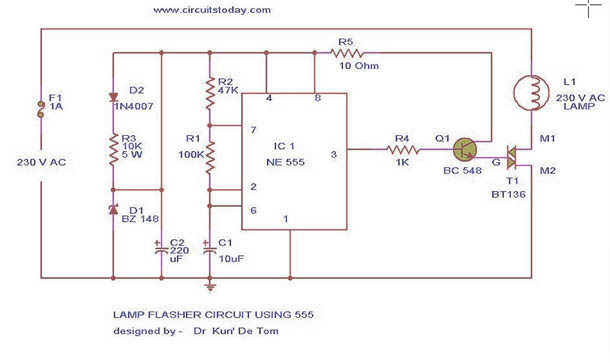
This circuit diagram represents a lamp flasher powered by mains electricity. It is capable of flashing lamps with a maximum power of 200 Watts at user-defined rates. The NE555 integrated circuit is configured as an astable multivibrator, generating the...