
DECUS Documentation

The DECUS divider module is designed to provide reliable signal conditioning and frequency division for rubidium oscillator outputs. Its compact size and versatile pin header configuration facilitate easy integration into various electronic systems. The module's ability to generate multiple marker signals makes it suitable for applications in timekeeping, frequency generation, and synchronization tasks. The three buffered ten megahertz outputs are particularly useful for interfacing with test equipment, ensuring signal integrity and robustness.
The design incorporates a hex inverter to condition the input signal, ensuring that it meets the operational requirements of the associated rubidium oscillator. The specified input voltage range is critical for maintaining optimal performance, and the use of an oscilloscope for verification ensures that users can confirm the module's correct operation before deployment. The flexibility to use a zener diode for higher voltage operation or to maintain functionality at lower voltages enhances the module's adaptability to different applications.
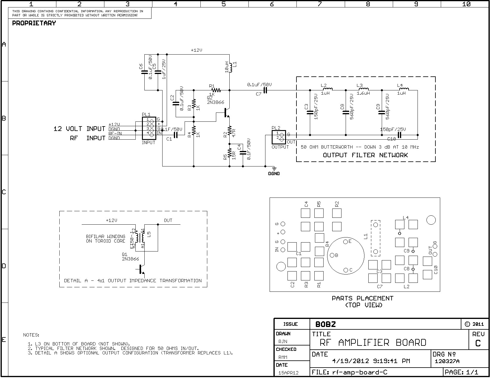
In summary, the DECUS divider module is a sophisticated solution for conditioning and dividing high-frequency signals, providing essential features that cater to both standard and specialized applications. Its design considerations, including current limitations and voltage requirements, are essential for users to understand to ensure reliable and effective operation in their specific use cases.The following describes the design, construction, operation and use of the DECUS divider module. Photo 2 shows a top view of the module and Photo 3 shows the bottom. The primary use of the module is to condition the 10 megahertz (MHz) signal from a rubidium oscillator such as the LPRO-101 or FRS-C units manufactured by EFRATOM Ball, Inc. The DECUS module divides the 10 MHz output from these units to produce marker signals at various frequencies. If you require a multiplied frequency output in addition to the decade divisor, you may be interested in the DECL module. If you have a FE-5680 rubidium reference, you may be interested in the FEBO module. The module`s conditioning circuit and divider chip can also be used for other applications requiring signal conditioning and dividing, but this usage is outside the scope of this document.
The schematic shows the components, circuitry and some operational restrictions for the module. The Parts List provides additional information about the components used to assemble the module. photo 2, the module measures approximately 1 1/4 by 7/8 inches (32 by 23 mm). Signal connections are provided on two 12-pin single row pin headers. The header connections are labeled "A" to "X" for easy reference. Header pins are spaced one tenth of an inch apart and the header rows are spaced 0. 6 inch apart. This allows the module to be used with in-line sockets or wired directly to a protoboard. outputs, ranging from one Hertz to one megahertz. The module also provides three ten megahertz buffered outputs for driving time base inputs of test equipment. Two buffer gates are uncommitted to allow any two of the outputs to be buffered or to allow buffering of an external signal (e.
g. , a lock indicator for an LPRO or FRS output). Divider outputs are driven by microprocessor port pins capable of sourcing or sinking up to 100 milliamperes each. The one Hertz output can directly drive an LED to act as an "active" indicator. These drive capabilities are limited by the choice of input voltage and the current limitations of the regulator, as noted in the Power section.
The input signal is applied between the module pins labeled "K" and "L" (ground), as shown in the schematic. The conditioning circuit is designed to be compatible with the LPRO-101 specifications with a typical input signal of 0.
55 Volts RMS (approximately 1. 5 Volts peak to peak). DECUS Photo 1 shows the typical input conditioning signals for a LPRO input. Note: The input may not operate reliably for signal inputs under one Volt peak to peak. Inputs as high as 6 Volts peak to peak have been used but are not recommended for routine operation. To verify the correct operation of the conditioning circuit, use an oscilloscope to observe the input signal between ground and pin 1 of the hex inverter. If the input voltage is within the range specified above, a 10 MHz square wave can be observed at pins "H", "T" and "V.
" Buffered versions of the conditioned signal appear at pins "J", "O" and "P" as shown in the schematic. schematic ). When using the zener, the input voltage applied to the module should be a minimum of 15 Volts. For direct operation at lower voltages, such as 5 Volts, the shorting jumper should be left in place (the factory-wired default).
To use the zener diode, cut the shorting jumper across the diode on the bottom side of the board. The addition of the zener drops the regulator input voltage to approximately 15 Volts. Note that operating the module at higher input voltages (e. g. , above 10 Volts) may significantly limit divider output currents, as noted below. Once the proper input voltage has been selected, configured and applied to pin "M", the operation of the regulator can be verified by measuring the voltage betweeen ground and the power pins of the ICs. For example, 3. 3 Volts should appear on pin 14 of the hex inverter and on pin 7 of the microprocessor. The measured 🔗 External reference
Related Circuits
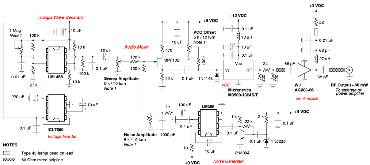
The amplifier is suitable for various projects to buffer and amplify outputs from devices such as Direct Digital Synthesizer (DDS) chips. It was initially designed to amplify the output of the 9833 DDS chip and is also intended for...
Note that the due dates for lectures 20-25 will be rescheduled to Wednesday at 1:00 PM. Download the notes for Topic 1: Basic Components (Listen to Dr. Stienecker) and Topic 2: Power and Connections (Listen to Dr. Stieneker). Students...

The PRUBY module provides a phase-locked loop (PLL) interface for rubidium frequency references, specifically the LPRO-101 and FRS-C products from EFRATOM Ball, Inc. This module conditions the 10 MHz signal from the reference and offers both a square wave...
The following describes the design, construction, operation, and use of the DECL (Decade PLL) module. The module incorporates a Phase Locked Loop (PLL) frequency multiplier and a frequency divider to generate various output frequencies based on an input reference...
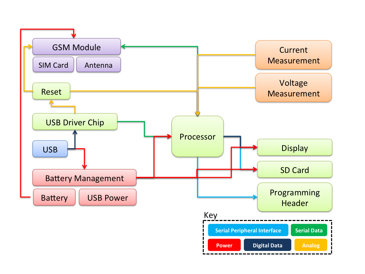
Datagoo is based on the ATMEGA328P microcontroller, widely used by hobbyists in various Arduino projects. It can be programmed via any computer with a USB port when paired with an FTDI FT232RL USB-Serial circuit. Cost-effectiveness and simplicity were prioritized...

The provided connections will enable configuration-free usage for most Arduino boards. Some Arduino boards, such as the Mega2560, may require custom configuration due to how the ports on the Atmel AVR microcontroller are mapped to the digital pins on...