
discussing output stage of square wave

The circuit design incorporates critical resistors that influence the performance and stability of the transistors and MOSFETs. The 10K resistors at the transistor bases serve to limit the base current, ensuring that the transistors operate within safe limits and preventing damage. Likewise, the 1K resistors at the collectors are vital for the proper operation of the MOSFETs, as they help manage the voltage and current flowing through the devices, ensuring reliable switching.
The oscillator section is designed to generate a waveform that can be adjusted based on the circuit's requirements. The output stage is responsible for amplifying this waveform and driving the transformer, which is crucial for applications such as power inverters. The design retains the integrity of the square wave format, which is known for its efficiency in driving inductive loads.
The inquiry about the diode junction and the potential removal of resistors R4, R5, R6, and R7 suggests a simplification of the circuit to enhance performance. By connecting the diode junctions directly through the 10K resistors, it may be possible to reduce complexity while maintaining functionality. However, caution is advised, as any changes made to the circuit, particularly in the secondary winding, could lead to unforeseen issues, including component failure and operational instability.
In summary, the circuit's performance hinges on the careful selection and placement of resistors and other components. Maintaining the integrity of the original design while making adjustments is critical to achieving the desired operational characteristics and ensuring reliability in the overall system.What about the 10K resistors at the bases of the transistors, and the 1K resistors at the collectors. Keep those with theTransistors when I move them, orget rid of them If the 10K resistors are not included the transistors will blow-off, without the 1K collector resistors the mosfets will not work.
so all of them are required. we are just interested in changing the waveform, which is solely connected with the oscillator section. The output stage which is responsible only for boosting the signals into the transformer windings, remains the same, just as it was with the square wave design. Hi Swag, one more question. On your circuit, at the Diode Junction, should I get rid of R4, R5, R6, R7 and just use the two 10K resistors, with the transistors.
Hi Swagatam, I followed your instructions to the letter and it still does not work. This time when I turned the Inverter ON it made a loud high pitched noise and blow one of the Mosfets. Sorry for the bad news. Hi Swagatam, here is a picture of the complete circuit on a PCB. The Square wave generator and PWM circuitare ontwo separate PCBs. I sure hope we can get this thing working. Quite unfortunate that its not working, you may directly connect the diode junctions through the 10K resistors of the square wave design, so R4, 5, 6, 7 are not required.
are you sure you are using exactly the same output stage set-up that was previously working with the square wave design I think you did some changes in the secondary winding. if that is true then that may be root cause of all the trouble. 🔗 External reference
Related Circuits
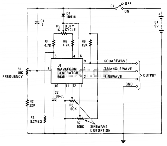
The circuit is designed around the Intersil 8038CC. The frequency range is approximately 20 Hz to 20 kHz, providing a tuning range of 1000:1 with a single control. The output frequency is determined by the value of capacitor C2...

The circuit diagram for a multiple output digital camera power supply using the MAX1802 is illustrated below. The MAX1802 chip features two buck converters and three boost converters. It accepts an input voltage range of 2.5 to 11V and...

The MAX2620 integrates a low-noise oscillator with two output buffers in a cost-effective, plastic surface-mount, ultra-small uMAX package. This device combines functions that are typically achieved with discrete components. The MAX2620 is designed for applications requiring precise frequency generation with...
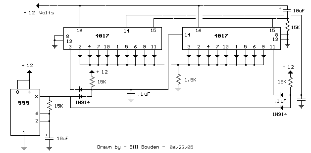
When power is applied, the 15K resistor and 10µF capacitor at pin 15 will reset the counters to a zero count, with pin 3 at +12V and all other outputs at zero. The two diodes (1N914) and a 15Ω...
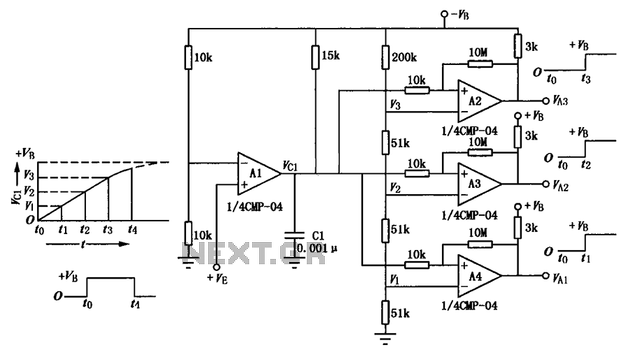
A multi-stage delay circuit is presented in this schematic. The operational amplifiers are configured as comparators. Operational amplifier A1 operates when the voltage at the inverting input exceeds + VE. As the voltage at the inverting input of operational...
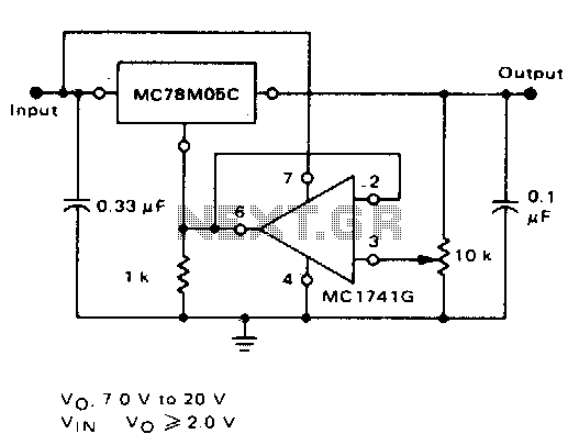
The inclusion of an operational amplifier facilitates the adjustment to higher or intermediate voltage levels while maintaining regulatory characteristics. The minimum voltage achievable with this configuration is 2 volts above the regulator voltage. The circuit employs an operational amplifier (op-amp)...