
Double transistor low noise of the preamplifier measured by high

The Bong ordinary differential amplifier circuit is a sophisticated configuration designed to enhance signal processing capabilities by converting voltage signals into current feedback. This circuit employs resistors R and Rl to achieve a voltage-current conversion, which is pivotal for maintaining signal integrity across various operating conditions. The operational amplifier within this circuit is equipped with a voltage divider that plays a crucial role in determining the feedback mechanism, effectively transforming voltage signals into a manageable current format.
The voltage gain of the circuit is a significant parameter, calculated using the formula A = (VRi) * (1 + Rl/Rs). This indicates that the gain can be finely tuned by adjusting the resistor values, allowing for a versatile range of amplification from 1 to 1000. Such flexibility is essential in applications where precise signal amplification is required, such as in sensor interfacing and audio processing.
A notable feature of this circuit is the arrangement of two transistors that connect at the base, which serves to minimize the common-mode input voltage. This reduction is crucial as it enhances the performance of the amplifier by mitigating the effects of noise and interference that can compromise signal fidelity. However, this modification also necessitates careful consideration of the operational amplifier's characteristics, as the typical assumptions regarding gain and bandwidth may not hold true under these conditions.
In addition, attention must be given to the collector drop resistance of the differential amplifier's transistors, specifically Ri and Rz, which are configured in series to facilitate offset adjustments. This adjustment is vital for eliminating any inherent offsets that could distort the output signal. If the circuit exhibits sufficient zero drift, it may be feasible to eliminate the VRZo component in a multistage amplifier setup, thus simplifying the design while maintaining performance. However, caution must be exercised, as neglecting this adjustment may lead to instability or oscillations in the output.
To further enhance stability, a phase compensation circuit may be integrated into the design. This circuit is critical for ensuring that the amplifier operates within a stable range, particularly at higher gains where phase shifts can lead to undesirable feedback loops. The selection of component parameters for this compensation circuit should be based on the minimum gain requirements, ensuring that the amplifier remains responsive without sacrificing stability.
In summary, the Bong ordinary differential amplifier circuit represents a refined approach to signal amplification, combining voltage-current conversion with adjustable gain and stability features. Its design considerations are essential for achieving optimal performance in various electronic applications. Bong ordinary differential amplifier circuit and the difference circuit is that it has made a voltage-current conversion circuit rPl constituted with R. And Rl o of the OP ampl ifier includes a voltage dividing, and then convert it into current feedback. Voltage gain of the circuit can be A! Type Health + VRi) (1, a Rioj R.) --- Rs calculated. If quad + v crown. About cricket oQ, according ugly s 33 2 ~ µ3kC!. 4 magnification may be in the range of l-l000 of the. Because the two-transistor Fr guard base connected - mine death o, they were neat sodium 3. 9V two pipe confidence vote, so that the common-mode input voltage is reduced, then the generic OP amplifier characteristics can not be used, should be noted o VRs differential amplifier transistor collector drop resistance Ri and Rz series for offset adjustment. If there is enough after the circuit zero drift, you can not VRZo in a multistage amplifier circuit to reduce the magnification if, it would have a vibration.
End, and therefore need to add a phase compensation circuit (mouth, and,.), Component parameters from the minimum gain decision stingy
Related Circuits
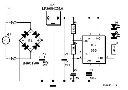
This article is relevant only to readers whose bicycle lights are powered by a dynamo. The regulations regarding bicycle lights in the United Kingdom are stricter than in many other countries, making dynamos a rarity in the UK. For...
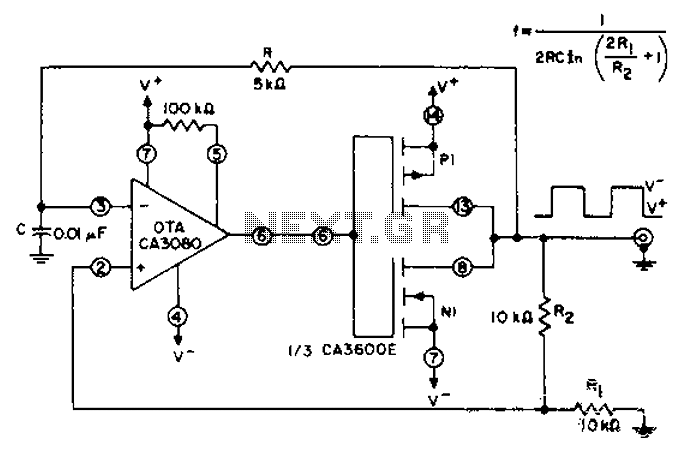
CA3600E array transistor pair and a reverse CA3080 operational amplifier are used together to provide precise timing and thresholds for the square wave. A typical static power consumption is 6mW. The CA3600E is a versatile integrated circuit that includes multiple...
Design a low-cost 4- to 20-mA receiver circuit for control loops using an analog-to-digital converter (ADC). The design of a low-cost 4- to 20-mA receiver circuit is essential in industrial applications for monitoring and controlling processes. This current loop standard...
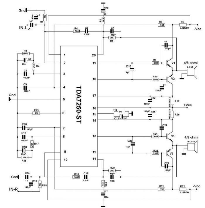
The TDA7250 audio driver, manufactured by SGS Thomson, can be utilized to design a straightforward high-power audio amplifier project with minimal external components. This audio amplifier can operate with either a 4-ohm or an 8-ohm load, delivering a maximum...
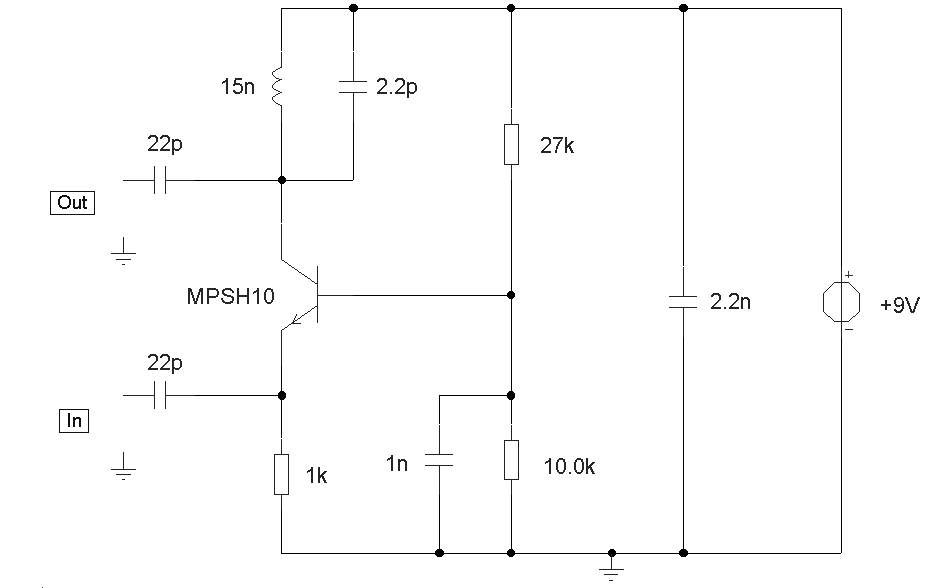
The circuit design aims to create a preamplifier for television systems that operates within the UHF frequency range of 450 MHz to 800 MHz. The preamplifier circuit is essential for enhancing weak television signals before they are processed by the...
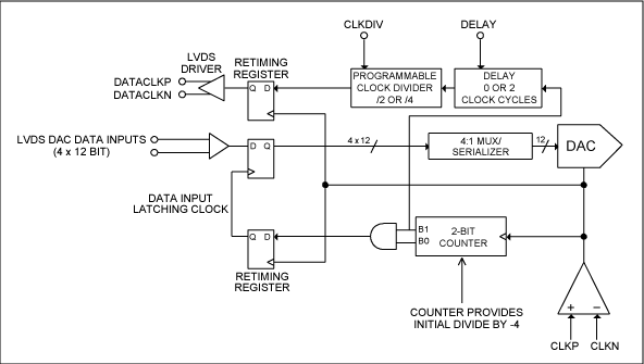
This application note provides insight into how to synchronize multiple high-speed DACs in transmitter applications. This document outlines the techniques and methodologies for synchronizing multiple high-speed Digital-to-Analog Converters (DACs) in various transmitter applications. Synchronization is crucial in systems where multiple...