
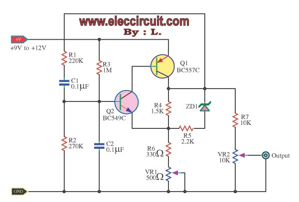
Dynamo Frequency Monitor

IC1 serves as the core component of a voltage comparison circuit, leveraging the characteristics of dual operational amplifiers to monitor voltage levels and dynamically control the charging of capacitors based on the frequency of the dynamo output. The operational amplifiers are configured in a comparator mode, which is essential for detecting when the input voltage crosses a specified reference level.
The first comparator, IC1a, plays a vital role in monitoring the charging state of capacitor C1. The reference voltage for this comparator is adjustable via potentiometer VR1, allowing for calibration to specific operational conditions. Resistors R4 and R5 form a voltage divider, ensuring that the reference voltage remains stable and suitable for comparison with the voltage across C1.
The output of IC1a (c) is crucial for determining the charging state of capacitor C2. When the output is high, indicating that the frequency is below the critical threshold, C2 receives charge through the forward-biased diode D2. The slow discharge of C2 through resistor R6 when the output is low ensures that the voltage across C2 (d) gradually decreases, providing a time-dependent response which is critical for the operation of the second comparator, IC1b.
IC1b compares the voltage across C2 against a set threshold defined by resistors R7 and R8. This comparison allows the circuit to determine whether to switch the power source from the dynamo to the battery, ensuring that the system can operate efficiently based on the dynamo’s performance.
The choice of operational amplifiers, such as the CA3240E, is pivotal due to their ability to operate effectively in single-rail configurations, ensuring that the output can reach ground level, which is necessary for the intended application. The use of a transistor like the ZTX300 for TR1 provides the necessary switching capability to manage the power sources effectively, enhancing the circuit's reliability and efficiency.
Overall, this circuit exemplifies a robust design that integrates voltage comparison, dynamic charging, and power management, making it suitable for applications that require efficient energy utilization from variable sources such as dynamos.IC1 is a dual operational amplifier. In this circuit each op-amp is used simply as a voltage comparator. When the voltage at the + input is higher than the voltage at the - input, the output goes high. When the voltage at the + input is lower than the voltage at the - input, the output goes low. The 8-pin package contains two of these comparators, IC1a and IC1b. IC1a is used to compare the voltage on C1 (b) against a reference voltage provided by the potentiometer VR1 and resistors R4 and R5. The idea is that when the dynamo output is below the critical frequency, C1 charges for long enough that for some of the time (b) is greater than the reference voltage, producing pulses on the output of IC1a (c).
On the other hand, when the frequency is above the critical frequency, (b) never exceeds the reference voltage, so (c) is always low. When (c) is high, C2 is charged through D2. When (c) is low, C2 slowly discharges through R6. The voltage on C2 (d) is compared against a reference voltage provided by R7 and R8 by IC1b. When the dynamo frequency is low and C2 is being periodically charged, (d) will be above the threshold and the output of IC1b (e) will be high.
When the dynamo frequency is high and C2 is not being charged, (d) will be below the threshold and the output of IC1b (e) will be high. This output is used to switch between the battery and the dynamo. Note: When selecting an operational amplifier, it is important to choose one that is designed for single-rail operation.
Other devices will not drive their output to 0v. One suitable device is the CA3240E. I used a ZTX300 as TR1. 🔗 External reference
Related Circuits
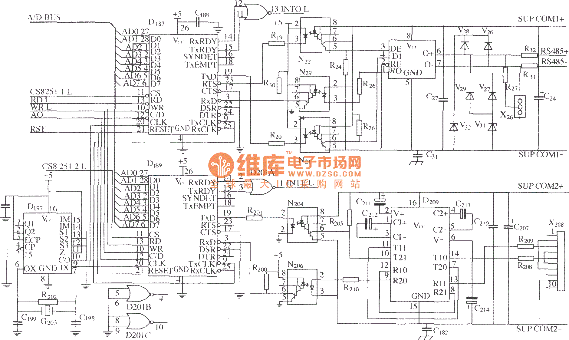
As shown in the figure, D187 is a UART with its RX/TX signals connected through optocouplers N21, N22, and N29, providing complete optoelectronic isolation for the RS-485 communication interface receiver/transmitter D28 and microprocessor D211. D197 serves as a generator,...
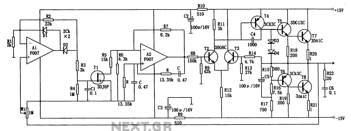
The low-frequency signal generating circuit demonstrates excellent performance characterized by stable operation, high output power, and minimal waveform distortion. It serves as an ideal source for low-frequency measurement signals. The circuit includes an operational amplifier (A) with a feedback...
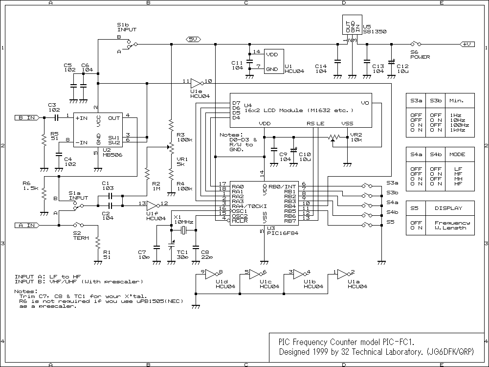
To achieve greater sensitivity, consider using the 74AC04 or 74HC04 in place of the 74HCU04 for component U1. While the 74AC04 and 74HC04 may offer improved performance over the 74HCU04, it is important to note that the frequency response...
The construction is nearly complete, and a circuit diagram has been created. The design has been finalized and documented on paper. The circuit diagram represents a critical stage in the development of an electronic project, serving as a blueprint for...
In a sine wave oscillator circuit, a thermistor and an incandescent lamp are often utilized to stabilize the output of the circuit at a fixed value. The resistance of... The sine wave oscillator circuit is designed to generate a continuous...
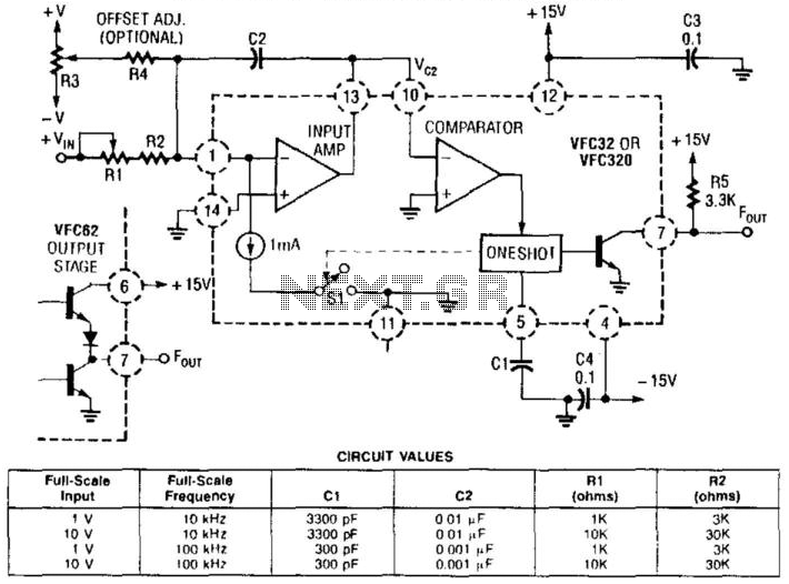
This voltage-to-frequency converter utilizes a Burr-Brown VFC 32 integrated circuit (IC) and requires minimal components. The circuit values are illustrated in the accompanying figure. This charge-balanced voltage-to-frequency (V/F) converter employs either a VFC32 or a VFC320 IC. The positive...