
Electronic pulse circuitry fishing

The SC3525A PWM controller is designed for various applications, including power supplies and motor control circuits, due to its versatility and efficiency. The error amplifier plays a crucial role in maintaining the desired output voltage by comparing the feedback voltage to a reference voltage. The configuration allows for precise control over the output characteristics.
Pins 5 and 6, responsible for timing, determine the frequency and duty cycle of the PWM signal. The timing capacitor and resistors connected to these pins set the oscillation frequency, which is vital for the operation of the circuit. The discharge terminal on pin 7 is essential for resetting the timing capacitor, ensuring that the system can cycle correctly.
The soft-start feature on pin 8 is particularly important in applications where inrush current could damage components. By gradually ramping up the output voltage, this feature protects the circuit during startup.
PWM input compensation on pin 9 allows for adjustments in the PWM signal to optimize performance based on load conditions. The signal input on pin 10 is the primary control input for the PWM signal, which modulates the output based on the desired performance characteristics.
Output A and output B, found on pins 11 and 14 respectively, can drive external components or circuits directly, providing flexibility in design. The bias voltage terminal on pin 15 ensures that the internal circuitry operates within specified voltage levels, while the reference voltage output on pin 16 provides a stable voltage reference for other components in the circuit.
The totem pole output stage enhances the ability of the SC3525A to drive power MOSFETs directly, facilitating efficient switching operations in high-power applications. This characteristic is essential for minimizing losses and improving overall system efficiency. The design of the SC3525A makes it a reliable choice for engineers looking to implement PWM control in their electronic designs.Circuit works: SC3525A for the US General Semiconductor PWM silicon chip, 1 foot of the error amplifier inverting input terminal, pin 2 is the error amplifier non-inverting input terminal, 5,6 feet for the timing of the end, the discharge end 7 feet, 8 feet for soft-start end, 9 feet for the PWM input compensation, 10 feet off the signal input, Il pin as an output a, 12 feet to the side, 13 feet for the output stage bias terminal, 14 feet output B, 15 feet for a bias voltage terminal access, 16 feet for the reference voltage output. Internal manifold with a totem pole amplifier circuit can directly drive the power MOSFET.
Related Circuits
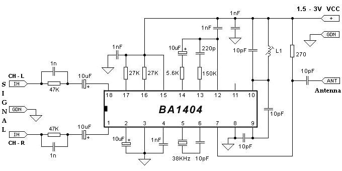
The BA1404 can be utilized to create a simple and effective FM stereo modulator electronic project. This BA1404 FM stereo modulator device operates within the FM broadcast band (75-108 MHz) and requires only a few common external components. The...
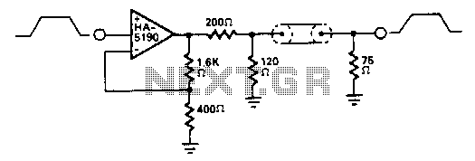
The HA-5190 can drive the 75-ohm coaxial cable with signals up to 2.5 V peak-to-peak without the need for current boosting. In this circuit, the overall gain is approximately unity due to the impedance matching network. The HA-5190 is a...

A portable CD player, radio, cassette player, a couple of microphones, and a PC sound card are connected to the inputs of an audio mixer. The output of the mixer is connected to a pair of active loudspeakers. The...
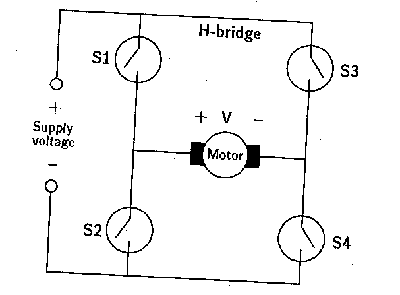
A microprocessor cannot drive a motor directly since it cannot supply enough current. Instead, an interface circuit is required so that the motor power is supplied from another source, with only control signals derived from the microprocessor. This interface...
The electronic tachometer frequency converter circuit operates by converting the input signal into a proportional current that can be measured by a pointer device. The electronic tachometer frequency converter circuit is designed to accurately measure the rotational speed of a...
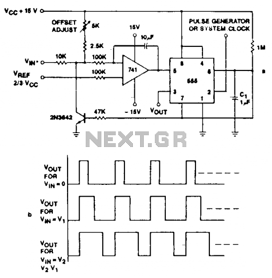
Accuracies better than 1% can be achieved with this circuit (a), and the output signals (b) maintain the original frequency, regardless of the input voltage. Voltage levels can be transformed into pulse durations by integrating an operational amplifier (op...