
Electronic Switch ON-OFF

The described circuit utilizes CMOS technology to create electronic switches that respond to touch or push-button activation. The fundamental components include NAND or NOR gates configured as an R-S flip-flop, which allows for the retention of a state after an input switch has been activated. In the configuration shown in Figure 1, pressing switch S1 sets the output at pin 3 to a high state (logic 1), maintaining this state until switch S2 is pressed, which then sets the output at pin 3 to low (logic 0) and the output at pin 4 to high.
To enhance the stability of the output states, a capacitor (C=100nF) can be connected in parallel with the respective switch. This capacitor serves to filter any transient signals that may occur when the switch is activated, providing a more stable logic level at the output. Figure 2 illustrates a CMOS inverter circuit where a resistor (R) is connected to the supply voltage, creating a high input state at the inverter. The output at pin 2 will be low (logic 0) until switch S2 is pressed, which pulls the input at pin 3 to ground, resulting in a high output state.
For applications requiring opposite logic behavior, the resistor can be connected to ground while the switch connects to the supply, reversing the logic states. This principle is consistent even when replacing the inverter with NAND or NOR gates, as shown in Figure 3.
To maintain a consistent output state after the switch has been released, it is advisable to implement a J-K or D flip-flop after the CMOS gates. This flip-flop will toggle its state with each activation of the switch, thus retaining the last state until the next activation. The circuit design allows for flexibility in component selection; switches can be replaced with contacts, and resistors can range from 100KΩ to 1MΩ when using push-button switches. For contact-based switches, a higher resistance value of 10MΩ is recommended to prevent unintended gate activation due to noise. Additionally, a 100nF capacitor may be placed in parallel with the contacts to mitigate noise issues and ensure reliable operation.Here we have three choices, with which we can make electronic switches that use our touch or pressing (push button). We thus exploit the very big resistance of entry, that present the gates CMOS. In the fig.1 we have two gates NAND or NOR (IC1), connected as R-S flip-flop. Just as we press the switch S1, the exit 3 it becomes [H], even it is maintained in this situation. To change the situation, it should we press switch S2. Now exit 3, takes price (L), reversely exit 4 becomes (H). In order to we maintain the situation that we want, we can connect at parallel with the corresponding switch, a capacitor C=100nF.
This entry will always drive the corresponding exit to logic (L), immediately afterwards the benefit of supply to the circuit. In the fig. 2, we have a circuit of inverter CMOS, in the entry of which is applied logic situation (H), from the resistance R, which the other end of, is in the supply.
Exit 2 has situation (L). When we press switch S2, in the entry of 3 IC2, we have situation (L), this it goes to the ground, the exit now becomes (H). This situations are maintained as long as we keep pressed switch S2 and they change immediately hardly the touch.
If we want opposite logic operation then it will be supposed we connect the resistance R, in the ground and switch S2, in the supply. The same logic we will have if we replace gate IC2, with a gate NAND or NOR, as it appears in the fig.
3, the result is the himself. Because the situation in the case of fig.1 and 3, does not remain constant and change when we pull our finger , in order to him we retain, it should we connect a J-K or D flip-flop as T, after the IC2 and IC3. Thus the flip-flop, will change situation, each time where we will touch the switch or will touch the contacts and him it will retain.
All the switches can be replaced with contacts, it is enough we replace also resistances R with the price of 10M?. The Resistances R when we use pressing switches can are, from 100K? until 1M?. Because when we use contacts instead of switches, the noise can turn on the gates of fig. 2 and 3, then can place a capacitor 100nF, parallel with the contacts. 🔗 External reference
Related Circuits
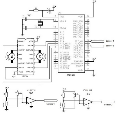
The electronic schematic of the Light Detector Robot can be divided into three main components: the sensor, the microcontroller, and the DC motor driver. The light sensor utilized in this design is a Light Dependent Resistor (LDR), which alters...
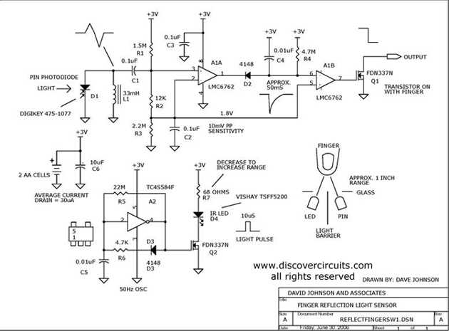
Infrared light reflected off a finger is used to activate this switch circuit. This circuit utilizes infrared (IR) light to detect the presence of a finger, allowing for a touchless activation mechanism. The core component of this circuit is an...
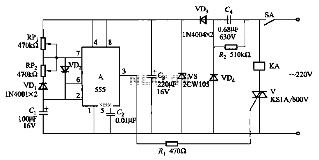
An automatic cycle switch circuit utilizing a 555 integrated circuit (IC) as the control element. It incorporates a capacitive step-down circuit and employs a bidirectional thyristor to control relays or loads with specific on and off timing. The circuit...
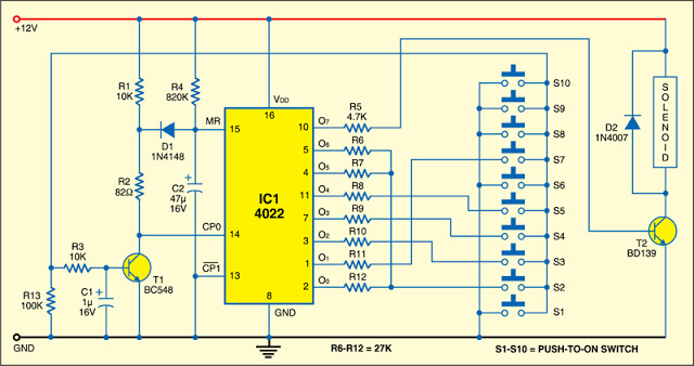
This 7-digit combination lock can be easily hard-wired for any combination that you choose. The circuit utilizes a 4-bit, divide-by-8 Johnson counter (IC1), ten push button switches, and an NPN transistor (T1). Upon power-on, capacitor C2 connected to pin...

The TDA2003 audio amplifier integrated circuit can be used to design a straightforward 10-watt power audio amplifier for a 2-ohm load or 4 watts for a 4-ohm load. The TDA2003 offers high output current capacity (up to 3.5A) and...
The concept involves mounting a microphone on a stick with an LED and designing a circuit that responds to loud noises detected by the microphone input (such as blowing) to turn off the LED. The schematic is straightforward, powered...