
Emitter-Coupled LC Oscillator

The described oscillator circuit operates based on the interaction between two transistors, Q1 and Q2, and an inductor-capacitor (LC) configuration. Initially, Q2 is activated, allowing the capacitor to discharge and charge the inductor, resulting in a rise in output voltage. The inductor's role is critical, as it temporarily stores energy in the magnetic field created by the current flowing through it. As the current through the inductor peaks, the voltage across it diminishes, which slows the conduction through Q2, thereby facilitating a transition to Q1.
The coupling of the emitters of Q1 and Q2 ensures that when Q1 begins to conduct, it effectively raises the emitter voltage, creating a feedback mechanism that prevents Q2 from drawing current. This feedback is essential for maintaining oscillation, as it allows for the inductor to continue charging the capacitor, thus sustaining the cycle of energy transfer. The point at which Q1 can draw all the current from the inductor, indicated by the output voltage reaching approximately 690 mV, is critical for the operation of the circuit.
As the inductor discharges, the current diminishes, leading to a drop in voltage, which ultimately causes Q1 to cease conduction. The transition to a negative output voltage activates Q2, allowing the cycle to repeat once the conditions are met for Q2 to start conducting again. The design of this oscillator takes advantage of the dynamic behavior of inductor-capacitor circuits, allowing for efficient energy transfer and oscillation at a specific frequency determined by the values of the inductor and capacitor. This type of oscillator can be utilized in various applications, including signal generation, timing circuits, and switching power supplies, where precise control of voltage and current is necessary.When the oscillator starts up, Q2 is conducting; the current comes from the capacitor, charging it until the voltage across it is large enough to get a current across the inductor. As the current across the inductor peaks, the output voltage rises (the inductor`s voltage difference is reduced), which causes the current across Q2 to slow down.
But the inductor isn`t done providing current, so the voltage across it (and the output voltage) rises as it charges the capacitor. Once the voltage turns positive, Q1 starts conducting, which raises the voltage of the two coupled emitters and prevents Q2 from conducting.
This keeps Q2 from sinking any current, which causes the voltage across the inductor to rise faster, since Q1 is not sinking much base current. Once the output voltage is at about 690mV, Q1 can draw all the current from the inductor, so the voltage across the capacitor (and inductor) peaks.
As the current across the inductor peaks, the voltage drops, which causes the Q1 base current to slow down. Eventually the output voltage goes negative, which shuts off Q1 and turns on Q2. Q2 doesn`t draw much base current, though, until the output voltage is at about -690 mV. At this point, the cycle begins again. 🔗 External reference
Related Circuits
Construct a Wien bridge oscillator that operates at 2.1 kHz and can be activated by a transistor. The inclusion of a transistor switch in the circuit allows for control of the oscillator's operation from a PIC microcontroller. However, during...
Colpitts oscillators are similar to the shunt-fed Hartley circuit; however, the Colpitts oscillator uses two series capacitors in its LC circuit instead of a tapped inductor. The connection between these two capacitors serves as the center tap for the...

Program an ATmega1284P using an AVR Dragon and the Arduino IDE. The mighty1284p library has been installed, and after writing the sketch, it is compiled using the Arduino IDE. The compilation process creates a hex file in a temporary...
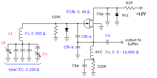
The circuit consists of two oscillators, both working at about 465 kHz. One uses an if transformer and the other uses an inductor (the search coil LI). The oscillators are coupled by a capacitor (10 pF). A beat note...
Examine a traditional Hartley oscillator circuit, and you'll note its trademark: a tapped inductor that determines the frequency of oscillation and provides oscillation-sustaining feedback. Although you can easily calculate the total inductance required for a given frequency, finding the...
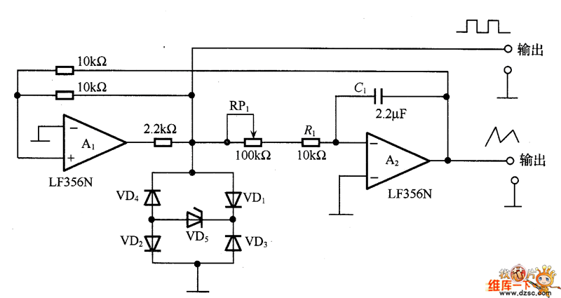
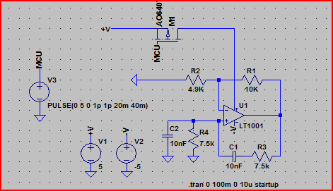
The circuit consists of a lag comparator with amplifier A1 and an inverting integrator A2. The charging and discharging time constant is determined by the integral resistors (R1 + RP1) and the capacitor C1. Diodes VD1 to VD5 form...