
Oscillator circuit diagram with triangle-wave/square wave output

The described circuit operates as a lag comparator integrated with an inverting integrator, which is essential for generating a specific output waveform in response to input signals. The lag comparator, represented by amplifier A1, is designed to compare input voltage levels and provide a corresponding output that reflects the delay in response. The inverting integrator, represented by amplifier A2, takes the output from the lag comparator and integrates it over time, producing a voltage that is proportional to the integral of the input signal.
The time constants for charging and discharging within this circuit are critically defined by the resistors (R1 and RP1) and the capacitor C1. The total resistance (R1 + RP1) determines how quickly the capacitor can charge and discharge, thereby influencing the overall response time of the circuit. A longer time constant results in a slower response, while a shorter time constant allows for a quicker response to changes in the input signal.
Diodes VD1 to VD5 are configured to form a limiter circuit, which serves to protect the subsequent stages of the circuit from voltage levels that exceed specified thresholds. This limiter circuit ensures that the output waveform remains within safe operating limits, preventing damage to sensitive components and maintaining signal integrity.
The maximum oscillation frequency of the circuit is closely tied to the switching rate of the amplifier. With a switching rate of 10V/µs, the circuit is capable of achieving a peak-to-peak output voltage of 20V. This relationship between switching rate and output voltage is crucial for applications that require rapid signal processing and precise control over voltage levels. The design considerations for this circuit are particularly important in high-speed applications where timing and voltage thresholds must be tightly controlled.The circuit is composed of lag comparator with A1 and inverting integrator A2, and the charging and discharging time constant is decided by integral resistors (R1+RP1) and the capacitor C1. VD1~VD5 form the limiter circuit. The maximum oscillation frequency is related to swicthing rate of amplifier, when swicthing rate is 10V/?
s, in order to get the 20V (p.. 🔗 External reference
Related Circuits

This design outlines a high impedance DC voltmeter circuit utilizing the uA741 integrated circuit (IC). The uA741 is configured as a non-inverting DC amplifier. The circuit incorporates negative feedback through a DC meter that requires 1 mA for full-scale...

The schematic circuit presented below illustrates an infrared transmitter. The infrared beam is emitted in a nearly line-of-sight manner towards another device equipped with an infrared receiver. The displayed waveforms represent the output voltages from two intermediate stages (purple...
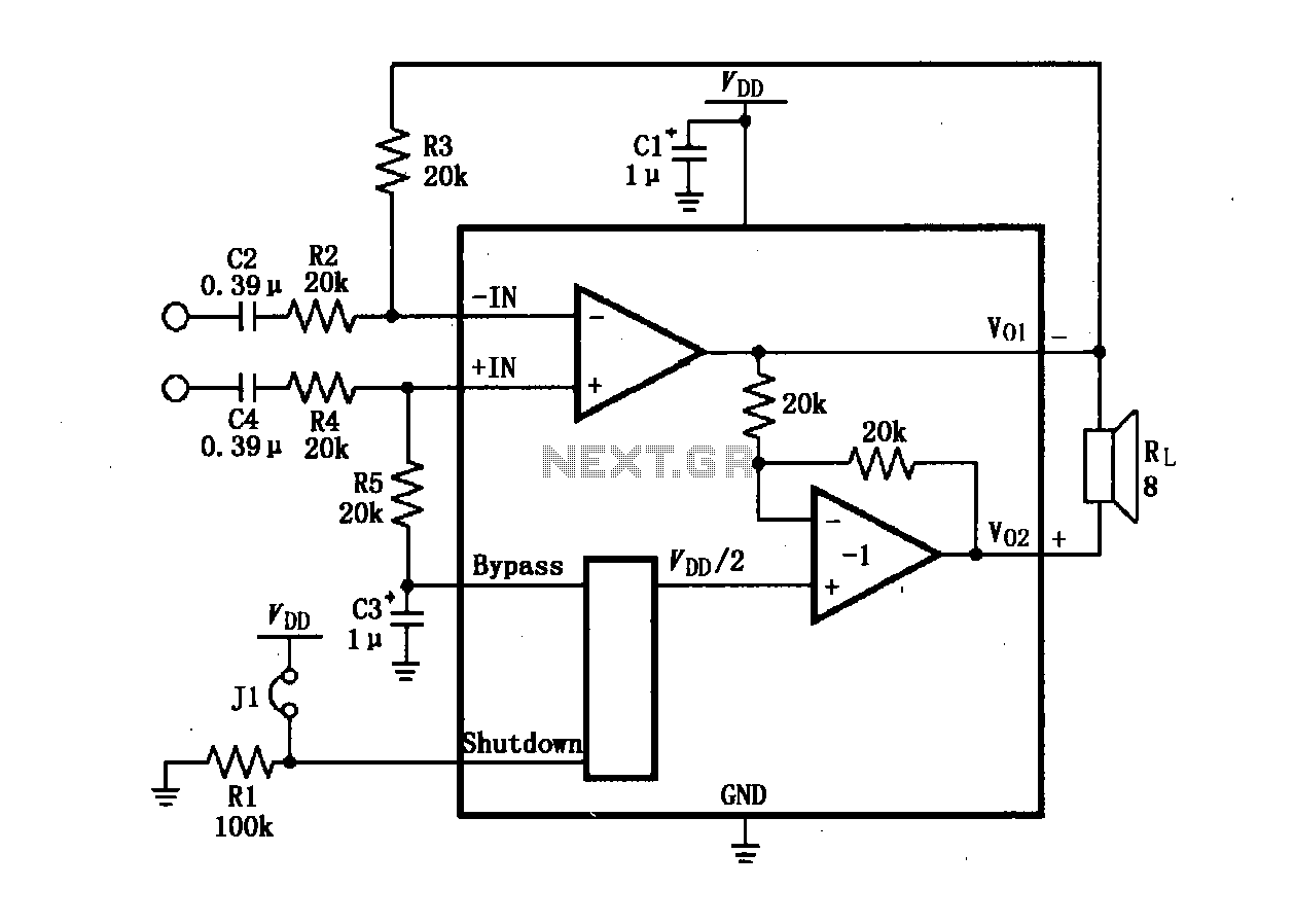
The LM4904 audio input differential amplifier circuit is presented. The audio signal is provided as a differential input to the +IN and -IN terminals. The LM4904 is a low-power audio input differential amplifier designed for high-performance audio applications. This circuit...
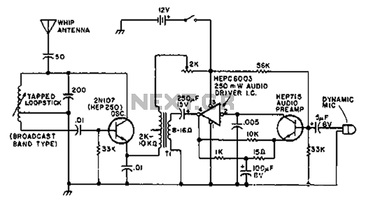
A circuit diagram of the T1 is a low-impedance output transformer, featuring a 5000-8 ohm resistor. The T1 low-impedance output transformer is designed to match the output of audio amplifiers to the impedance of loudspeakers, ensuring optimal power transfer and...
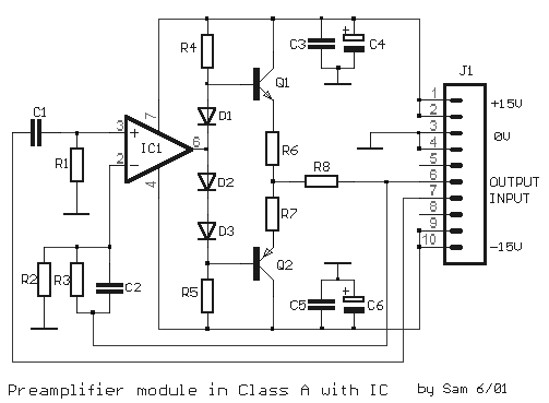
The circuit is based on a single operational amplifier integrated circuit designed to produce a modular preamplifier that operates in Class A configuration. The modular preamplifier circuit utilizes a single operational amplifier (op-amp) integrated circuit, which serves as the primary...
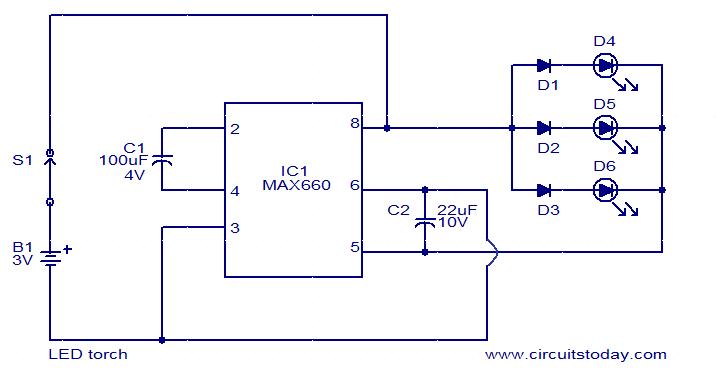
This circuit is a simple LED torch utilizing the MAX660 integrated circuit from MAXIM semiconductors. The MAX660 is a CMOS monolithic voltage converter IC capable of driving three bright white LEDs connected in parallel to output pin 8 of...