
Energy Saver Relay Coil circuit and explanation

This circuit is designed to optimize the operation of a relay by reducing the hold current once the relay is actuated, thereby minimizing heat generation and energy loss. The relay is actuated initially with full voltage to ensure reliable activation. The reduction of the hold current to approximately 50% of the initial value is achieved through a combination of resistors, capacitors, and transistors, which form a delay network.
The relay coil current, denoted as I, is critical for determining the resistance R3, calculated using the formula R3 = 0.7 / I. This relationship ensures that the resistance is appropriately sized to allow sufficient current to flow during activation while limiting the current during the holding phase. The charging time for the capacitor C1 is defined by the equation Charge time = 0.5 * G— R2 * G— C1, where G represents the gain of the circuit. This equation is essential for tailoring the timing characteristics to the specific relay being used.
To prevent the relay from being re-energized too quickly after being turned off, a delay is introduced. The capacitor C1 should be kept as small as possible to minimize the delay while still allowing a practical minimum of about 5 seconds for the relay current to stabilize. This timing can be adjusted based on experimental results to achieve the desired performance.
The role of capacitor C2 is to provide a brief surge of full supply voltage across the relay coil, ensuring rapid relay activation. The transistor T2, in conjunction with the delay network formed by C1 and R2, governs the flow of current through the first transistor T1 and the resistor R3, effectively controlling the hold current.
Diode D2 is employed to discharge C1 when the control voltage is low, ensuring that the capacitor is reset for the next cycle. The discharge time for C1 is approximately one second, allowing for a controlled return to the initial state. Additionally, diode D1 aids in the rapid discharge of C1, facilitating a quick response in the circuit.
The described relay operates at a specification of 12 V with a resistance of 400 ohms, making it suitable for various applications where reduced heat generation and energy efficiency are desired. All component values provided are for reference and should be adjusted according to the specific requirements of the application.Some relays will become warm if they remain energized for some time. The circuit shown here will actuate the relay as before but then reduce the hold` current through the relay coil current by about 50%, thus considerably reducing the amount of heat dissipation and wasted power. The circuit is only suitable for relays that remain on for long perio ds. The following equations will enable the circuit to be dimensioned for the relay on hand: R3 = 0. 7 / I Charge time = 0. 5 G— R2 G— C1 Where I is the relay coil current. After the relay has been switched off, a short delay should be allowed for the relay current to return to maximum so the relay can be energized again at full power. To make the delay as short as possible, keep C1 as small as possible. In practice, a minimum delay of about 5 seconds should be allowed but this is open to experimentation.
The action of C2 causes the full supply voltage to appear briefly across the relay coil, which helps to activate the relay as fast as possible. Via T2, a delay network consisting of C1 and R2 controls the relay coil current flowing through T1 and R3, effectively reducing it to half the pull in` current.
Diode D2 discharges C1 when the control voltage is Low. Around one second will be needed to completely discharge C1. T2 shunts the bias current of T1 when the delay has elapsed. Diode D1 helps to discharge C1 as quickly as possible. The relay shown in the circuit was specified at 12 V / 400 ohms. All component values for guidance only. 🔗 External reference
Related Circuits

A simple IF AGC signal with a wide dynamic range and excellent linearity characteristics may be composed of two chips: the TL026C T1 voltage control amplifier IC and the LT1014 (or any other similar basic quad op amp device). The...

Fluorescent tube light circuit of an inverter that uses a single transistor and a single transformer. This type of inverter can be made in various configurations. The fluorescent tube light circuit described utilizes a basic inverter design that incorporates a...
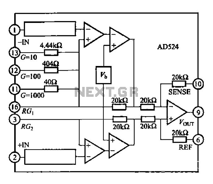
The AD524 is a low-drift instrumentation amplifier characterized by a drift voltage of 0.5 mV and a maximum drift of 25 mV at room temperature. It has low noise performance with a noise level of 0.3 mVp-p in the...
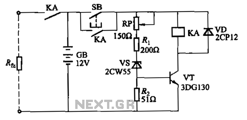
Deep discharge of a battery can lead to plate curing, which shortens the battery's lifespan. To prevent this, a discharge protection device can be implemented. The circuit diagram illustrates this mechanism. When the battery voltage falls to a predetermined...
Leo Esaki invented the tunnel diode in 1957 while working at Sony (then known as Tokyo Tsushin Kogyo). Tunnel diodes feature a very narrow, heavily doped p-n junction approximately 10 nm wide, which exhibits a broken bandgap. This configuration...
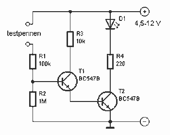
This little guide for every electronics tester would actually have to lie in the toolbox. You can have components such as resistors, capacitors, diodes, etc. of testing. T1 and T2 form a Darlington. Therefore only need a small base...