
Extensible Multiple Device Programmer 3

The power supply circuitry is designed to ensure safe operation by isolating high voltage AC from the low voltage DC components. The use of a wall wart power supply minimizes the risk of high voltage exposure on the board. The addition of a resettable polyswitch fuse enhances safety by automatically disconnecting the circuit in the event of a short circuit, which is a critical feature in protecting sensitive components.
The linear voltage regulators (VR1-VR5) provide a straightforward method of voltage regulation, albeit at the cost of energy efficiency. Each regulator is configured to provide a specific voltage output necessary for different components on the board. The choice of tantalum capacitors is strategic, as they offer low equivalent series resistance (ESR), which is beneficial for maintaining stable voltage during transient loads.
The communication interface of the EMDP3 board is robust, supporting both RS-232 and RS-422 standards. The dual communication paths allow for flexibility in connecting to various host systems, and the level shifting circuitry ensures compatibility between different voltage levels, which is essential for reliable data transmission. The use of OR gates (U9A and U9B) facilitates the selection of signals from multiple sources, allowing for effective communication between the master and slave microcontrollers.
The initialization sequence is critical for proper functionality. The coprocessor's control during startup ensures that the low-voltage processor is reset before any operations commence, preventing potential issues caused by uninitialized states. The subsequent level shifting ensures that signals are appropriately adjusted for the operating conditions of the microcontrollers.
Overall, the design prioritizes safety, functionality, and compatibility, making it suitable for various applications requiring serial communication and precise voltage regulation. The architecture reflects a well-thought-out approach to handling power and data, ensuring reliable performance in its intended use cases.The power supply uses a Underwriters Labratory ® approved "wall wart" to provide 24VDC of power. This means that the base board does not have any 110 AC or such voltages running around on it. The power comes in on either N1 (on board) or N3 (off board). The power switch can either be on board at SW1 or off board as SW2 through connector N2. A rese ttable polyswitch fuse is used to deal with short circuits at F1. D1 is a shorting diode that should trigger F1 if somehow a VAC power source gets plugged into N1 or N3. The rest of the power supply a series of inexpensive linear voltage regulators, VR1-VR5, that step the voltage from 24 volts, to 18 volts, to 12 volts, to 8 volts and finally to 5 volts.
All of these supplies are used elsewhere on the board except the 18 volt one, which is used to keep the 24 volt regulator, VR1, from disapating too much heat. The capacitors are tantalum for their low series resistance. This design will not win any energy conservation awards, but since the EMPD3 should spend 99% of its time turned off, there should be no real complaints.
Finally, green LED D2 lights up to indicate that the device is turned on. The EMDP3 is a board that uses standard serial communcations protocols. Connector N6 is used connect to a DB9 port on a host computer that uses RS-232 voltage levels for signalling. U7 in conjunction with C7 through C10 converts the RS-232 levels to 5 volt levels. Connector N7 uses a RJ45 jack to provide RS-422 using SimpliciNet pin outs. The nifty DS8921AT at U10 provides RS-422 to 5 volt signalling level conversions. U9A OR`s the recevied signal from U7 or U10 and forwards the signal to the slave microcontroller (U1), the master microcontroller (U2), and to some gating circuitry that potentially gates the signal onto one of the bi-directional bus lines.
U9B OR`s the transmit signals from the slave microcontroller (U1), the master microcontroller (U2), and through some gating logic with U8, potentially one of the bi-directional bus; the OR`d signal is forwarded to both the RS-422 connector and RS-232 connector. U1 is low voltage processor is a low-voltage PIC16LF877. This microcontroller has direct access to all 30 of the bidirectional lines. The remaining two lines are LVPRX for serial data recieve, LVPTX for serial data transmit. The adaptor boards can be connected to the bus via the 37-pin female D connector N4. Upon startup, the coprocessor is in charge. It immediately asserts LVPRESET# to force the low voltage processor into the reset state. Eventually, it will get around to setting VIO to the correct voltage and will release LVPRESET#. After that, the low voltage processor initializes itself and forces the bus lines to high impedance. Next, the programming algorithm is downloaded over the serial lines LPVRX and LVPTX. All level shifting from VCC (5 volts) to VDD (2 to 5 volts) is done by level shifting IC`s U11 through U14.
U11 and U12 are "up shifters" that take signals from VDD levels up to VCC levels and U13 and U14 are "down shifters" that take signals the opposite direction. The only c it will get around to setting VIO to the correct voltage and will release LVPRESET#. After that, the low voltage processor initializes itself and forces the bus lines to high impedance. Next, the programming algorithm is downloaded over the serial lines LPVRX and LVPTX. All level shifting from VCC (5 volts) to VDD (2 to 5 volts) is done by level shifting IC`s U11 through U14.
U11 and U12 are "up shifters" that take signals from VDD levels up to VCC levels and U13 and U14 are "down shifters" that take signals the opposite direction. The only chip that actually operates at VDD levels is U1, the slave microcontroller. Everything else is immediatehip that actually operates at VDD levels is U1, the slave microcontroller.
Everything else is immediately shifted up into the VCC level domain where any supsequent manipulation occurs. The reason for 🔗 External reference
Related Circuits
C1 is a charge pump capacitor. This works as a voltage doubler. When TxD is negative voltage, C1 is charged through D7 from GND. If TxD carries out turn-on, since it will become positive voltage, the voltage charged in...
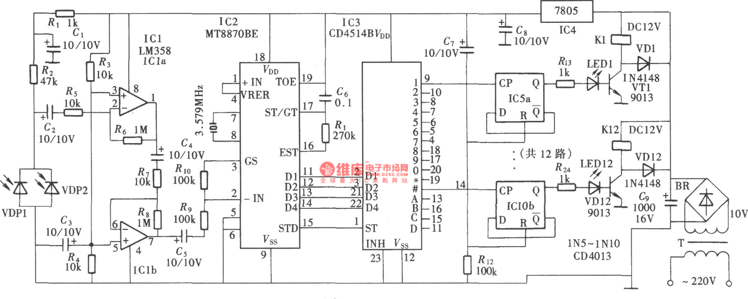
The DTMF codec stands for dual-tone multi-frequency codec. The multiple-channel infrared remote control switch circuit that incorporates the DTMF is depicted in the figure. It consists of an infrared remote control signal emitter, an infrared receiving signal amplifier, a...
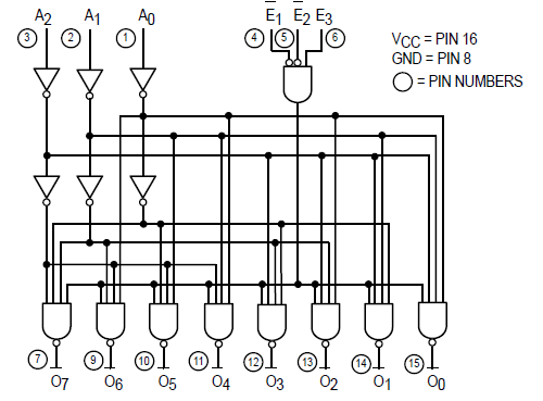
The Motorola SN54/74LS138 is recognized as a 1-of-8 decoder or demultiplexer, specifically engineered for high-speed bar memory chip select address decoding. The accompanying diagram illustrates the logic configuration of the SN54/74LS138 demultiplexer. According to the SN54 datasheet, the multiple...
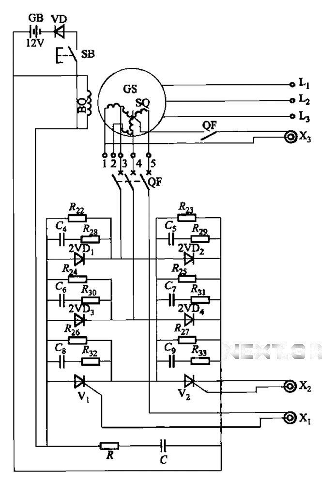
The setup is connected to separate stator windings of a harmonic generator, which leads to a thyristor rectifier supply for the third harmonic voltage, positioned after the motor field. The output voltage varies with changes in the winding harmonics...
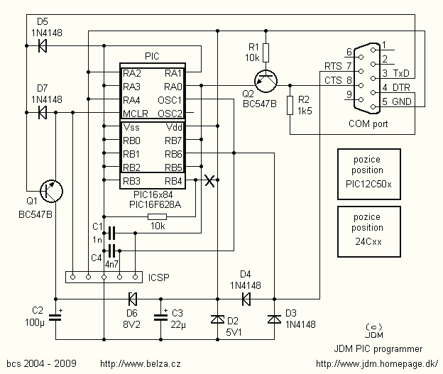
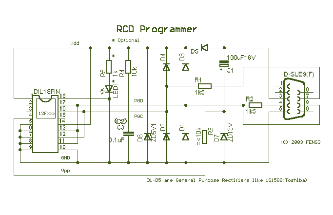
In the article you will find a description of the universal PIC programmer, which suggested the involvement of Jens Madsen Dyekjar. Program allows districts PIC12C5XX, 12C67X, 16C55X, 16C61, 16C62X, 16C71, 16C71X, 16C8X, 16F8X, serial EEPROM 24Cxx. It allows to...

These are simple AVR programmers. I designed and built four different programmers for various environments: LPT controlled parallel programmer, LPT controlled ISP adapter, COM controlled ISP adapter, and COM controlled generic SPI bridge. Additionally, COM controlled adapters can be...