
fitting a circuit scheme to a simpler mode
The circuit design primarily focuses on simulating the electric field within a gas-filled discharge gap, which is a critical aspect of various applications in plasma physics and high-voltage engineering. The components specified, such as capacitors, resistors, and inductors, are selected to create a resonant circuit that can efficiently generate high-frequency oscillations necessary for sustaining the discharge. The half-bridge configuration of the MOSFETs allows for effective switching, which is crucial for controlling the power delivered to the load.
The choice of a programmable logic device for control indicates a sophisticated level of automation and adaptability in operation, allowing for real-time adjustments based on system feedback. The high voltage step-up transformer plays an essential role in increasing the voltage to the desired levels for discharge initiation, while the parasitic capacitance is an important consideration in the design to mitigate losses and ensure stability during operation.
Safety measures are paramount in the design and operation of such high-voltage systems. The inclusion of galvanic isolation and the specification of experienced personnel for operation highlight the potential hazards associated with high voltage and electromagnetic interference. The circuit's design should also incorporate protective features, such as overvoltage protection and emergency shutdown mechanisms, to enhance safety during operation. Proper grounding and shielding techniques should be employed to minimize the impact of electromagnetic interference on nearby sensitive equipment.Simulate the electric field within a gas filled discharge gap generated by a radio frequency voltage generator. The circuit, provided to me by the experimenters somewhat far away, is given in the second picture below.
(Numerical values: $C1 = 22 nF=2. 2cdot 10{-9}, R1 = 2 Om, L1+L2 = 8 mu H=8. 0cdot 10{-6}, C2 = 3. 4n F=3. 4cdot 10{-9}$ [transformer parasitic capacitance]$, R2 = 100 MOm=108 Ohm, R3 = 1 Om, L3 = 100 nH=10{-7} H. $ Moreover, it`s running at 1MHz, sinusoidal, about $10kV$. ) $$=left(R_1+i omega (L_1+L_2)-ifrac{1}{omega C_1} ight)+left(R_3+R_{Gap}+i omega L_3 ight)frac{1}{1+(i omega C_2)left(R_3+R_{Gap}+i omega L_3 ight)}$$ I have no idea if it`s of relevance, but I can post the text of the manual of the generator, which I also have, but which isn`t really written in my language.
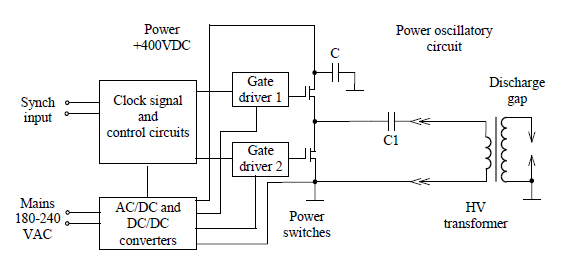
I have no idea how the picture even corresponds to the question above. The letter symbols seem a little off. So if the following doesn`t make any sense, then ignore it and just take the question above this at face value. "This generator simplified block diagram is presented on Fig. 5*` (the third picture). Clock signal generator, protect and control circuits are realized by using programmable logic device(PLD) Xilinx XCR32256XL.
This chip configuration(and generation parameters) could be changed in-system by special JTAG (Joint Test Action Group)-programmer. Control signal are boosted by gate drivers and gone to the power switch gates. The converter is designed as half-bridge circuit using MOSFET(Metal-Oxide-Semiconductor Field Effect Transistor) switches and fed by voltage up to 400 VDC.
Power oscillatory circuit, included elements C1 and high voltage step-up transformer having loss inductance L and parasitic capacitance C2, forms output voltage. In fire mode this circuit part can be simulated as two coupled oscillators; one of them consists of L and C2 and has resonance frequency about 1 MHz.
As a result, output voltage will increase fast, have sinusoidal-like shape and reach breakdown level of load. After discharge gap breakdown, in limit mode, capacitance C2 is shunted by small plasma impedance and we can ignore its influence on power oscillation.
Resonance of power oscillatory circuit in this mode will be defined by elements L and C1 and resonance frequency value will be less significantly than clock signal frequency(~1MHz). Output voltage will decrease a lot, its shape is changed to near triangle and power supply passes to limit mode.
Powerful 1. 3 kW capacitor charging module is used to feed RF converter circuit. It has galvanic isolation from mains and adjustable output voltage. Control circuits and gate drivers are fed by auxiliary AC/DC and DC/DC supplies. External synch signal is transferred by digital isolator, it has standard 50 Ohms impedance, active level is HIGH (+5 Vampl). Control signal is inactive if input connector is not jointed. " I also don`t actually know where the voltage they measure (which is supposed to be 10kV) is taken from in the circuit.
Maybe the pictures plainly say it, but I can`t read it. "High output voltage (up to 25 kV) and high level of electromagnetic interferences require highly experienced personnel to operate with generator. Careless use may be cause of electrical shock, health hazard, malfunction or even damage of nearby equipment.
" 🔗 External reference
Related Circuits
This three-band equalizer circuit is an active filter network designed for bass, midrange, and high audio frequencies. It utilizes the LM833 operational amplifier from National Semiconductors. The output of this three-way graphic equalizer is intended to be DC coupled;...

This is a basic overview of the LM35 temperature sensor, which is interfaced with an operational amplifier (op-amp) to boost its output. The LM35 provides a high output voltage when it detects high temperatures. The output can be utilized...
The charging circuit features adjustable voltage output settings, allowing for regulation of the charging voltage supplied to the battery. The use of a potentiometer facilitates precise voltage management, with adjustments possible down to the millivolt range. Refer to the...
This is a switch-selectable dual output version of a previous design from 2007, utilizing a field-programmed EPROM to generate two versions of the ringing sequence. The AC mains voltage is stepped down to approximately 10 V AC and then...
Construct a Wien bridge oscillator that operates at 2.1 kHz and can be activated by a transistor. The inclusion of a transistor switch in the circuit allows for control of the oscillator's operation from a PIC microcontroller. However, during...

This circuit diagram represents a low-cost metal detector utilizing a single transistor circuit in conjunction with an old pocket radio. It operates as a Colpitts oscillator functioning within the medium band frequency range, with the radio tuned to the...