
Five uses tri-state audio logic pen (CD4066 555) circuit diagram
")
The circuit operates by leveraging the CD4066, a quad bilateral switch, which allows for the routing of audio signals based on control inputs. Each of the four switches can be independently activated, enabling multiple audio paths to be selected. The multivibrator configuration using the 555 timer provides a square wave output, which can be used to toggle the control pins of the CD4066, thus determining which audio path is active at any given time.
Resistors R7, R8, and R9 are configured to set the timing characteristics of the multivibrator, while capacitor C1 serves to stabilize the timing intervals. The frequency output from the multivibrator can be adjusted by varying the resistance values or the capacitance, allowing for flexibility in the audio signal processing.
Overall, this circuit design is suitable for applications requiring the selective routing of audio signals, enabling functionalities such as audio mixing or switching in various electronic devices. The combination of the CD4066 and the 555 timer provides a robust solution for managing audio signals with precision and reliability.Five uses tri-state audio logic pen (CD4066, 555) circuit diagram is shown as the chart. The circuit is mainly composed of the multivibrator, the four-way switch CD4066 (IC1) and the gate circuit composed of some RC components. Multivibrator is composed of the 555 (IC2) and R7, R8, R9, C1, and its frequency is controlled by IC1-3 on-off state.
🔗 External reference
Related Circuits
The schematic diagram below illustrates a typical 1.5V flasher circuit using the LM3909. The LM3909 is a monolithic oscillator designed specifically for flashing Light Emitting Diodes (LEDs). The LM3909 flasher circuit operates at a low voltage of 1.5V, making it...

Using an old moving coil instrument, it is easy to create a simple voltmeter that indicates the status of a telephone line at a glance. The circuit's high input impedance allows it to be permanently connected to the line,...
The first application has to be a stereo power amp, since that's what I built using two prototype modules. The reasons for this choice are twofold - a good high powered stereo amp is always useful, and it was important...
This bench power supply features three solid-state DC power supplies. The first supply provides an output of 1.5 to 15 volts at 1 ampere. The second supply offers a range of -1.5 to -15 volts at 1 ampere. The...

The simple pulse width modulation circuit is illustrated in the figure. It utilizes an operational amplifier to create a multivibrator, resulting in a symmetrical oscillation output signal with a duty cycle of 50%. By adjusting the external threshold voltage,...
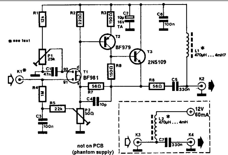
A whip antenna measuring between 30 to 50 cm is capable of receiving signals from 10 MHz to over 220 MHz. The circuit incorporates a BF981 dual-gate MOSFET (T1), which offers low noise characteristics, high input impedance, and enhanced performance. The...