
FOUR STATION TWO WAYl

The described circuit encompasses multiple functionalities, including timing, frequency multiplication, and signal conditioning. The timing circuit utilizes a unijunction transistor and silicon-controlled rectifier to manage voltage application to a load with a significant delay range. The frequency multipliers and harmonic generators are designed to manipulate input waveforms, producing a controlled harmonic output while filtering even harmonics through differential signal processing. The feedback mechanism is crucial for protecting the circuit from high-voltage transients, thereby enhancing reliability when interfacing with inductive loads. The design is robust, covering a wide operational temperature range and allowing for component tolerance adjustments, ensuring consistent performance in varying conditions. The integration of a universal asynchronous receiver-transmitter enables seamless communication between devices, facilitating simultaneous data transmission and reception. Furthermore, the programmable flat-pulse generator and clamp amplifiers provide versatile applications in digital signal processing, showcasing the circuit's adaptability across various electronic systems.Timing interval is initiated by applying power, and is determined by RT-CT. At end of interval, unijunction transistor triggers silicon controlled rectifier, to apply essentially full supply voltage to load. Delay range is from 0. 4millisec to 1 minute. - Transistor Manual, Seventh Edition, General Electric Co. 1964, p 321. (View) Addition of silico n unijunction transistor Q3 to conventional mono stable mvbr expands time delay two orders of magnitude. -M. P. Humblet, Unijunction Transistor Multiplies Monostable `s Pulsewidth, Electronics, 35:26, p 74-75. (View) This simple circuit acts as a frequency multiplier, which converts any sloped input waveform into a distorted output waveform, whose frequency spectrum is marked by a rich harmonics content.
The input frequency does not disappear from the spectrum, however. When a pure sine-wave input signal is applied, the circuit generates odd harmonics only. The push-pull outputs of comparators IC1b and IC1a then supply differential signals to adder IC2, which cancels out even-numbered harmonics. For different mark/space ratios of the output signals, as set with P1 and P2, the harmonic spectrum changes.
A duty factor of 0. 25, for instance, will cause the circuit to supply the second, sixth, and tenth harmonics, but not the fourth one. The spectrum function is then written as sin x/x. The reference levels for the input comparators determine the output waveform. The desired degree of distortion of the input waveform is, therefore, adjusted with the two presets. R2 and R3 should be matched to within 1 percent. (View) Feedback from collector to base of power transistor through C1 and R2 protects device from destructive transients generated when inductive load such as solenoid is turned off.
Alternative use of diode CR2 or CR1-R1 across coil would limit voltage transient but would increase solenoid release time. -D. Thomas, Feedback Protects High-Speed Solenoid Driver, EDN Magazine, Jan. 1, 1971, p 40. (View) Basic design procedure is given. Circuit shown operates over temperature range of -55 to +55ƒ with input frequency of 250 kc. -Texas Instruments Inc. , Transistor Circuit Design, McGraw-Hill, N. Y. , 1963, p 377. (View) Circuit for microelectronic application allows use of most suitable substrate for each component.
-J. Eimbinder, Multichip Circuits Get Off The Ground, Electronics, 37:25, p105-107. (View) Design procedure is given in 52 steps for manufacturability and long-term reliability, making full allowance for component tolerances, voltage fluctuation, and collector output loading. - Transistor Manual, Seventh Edition, General Electric Co. , 1964, p 189. (View) Fan-out of conventional flip-flop is quadrupled by driving bases of amplifiers Q1 and Q2 directly from emitters of Q3 and Q4.
-D. J. Grover, Modified Flip-flop Quadruples Fan-Out, Electronics, 38:26, p 67-68. (View) Permits use of universal asynchronous receiver-transmitter with model 33 Teletype so keyboard can send and printer can receive at same time. Transmitter interface provides 20-mA current for mark or 1 and open circuit for space or 0. Receiver senses closed contact for mark or 1 and open contact for space or 0. Extra inverters are added to make codes correspond so 1 from UART is read as 1 by Teletype. Designed for 110-baud rate. -D. Lancaster, TV Typewriter Cookbook, Howard W. Sams, Indianapolis, IN, 1976, p 162-164. (View) This circuit provides a programmable flat-pulse generator with TTL input and up to 24 V p-p output with a 2500-V- s slew rate.
Clamp amplifiers are useful as protective buffers for A/D inputs, as programmable flat-pulse-forming amplifiers, and as amplitude modulators. Because VH and VL clip in the in-put stage and have input bandwidths comparable to the signal inputs, they can also be used in simple circuitry to generate the positive or negative absolute value of input signals (i.
e. , full-wave rectify them). (View) Developed 🔗 External reference
Related Circuits

The circuit in Fig 1 provides both 3.3V and 5V power to transitional circuits that utilize both newer 3.3V devices and older 5V devices. Additionally, due to the regulator... The circuit illustrated in Fig 1 is designed to accommodate the...
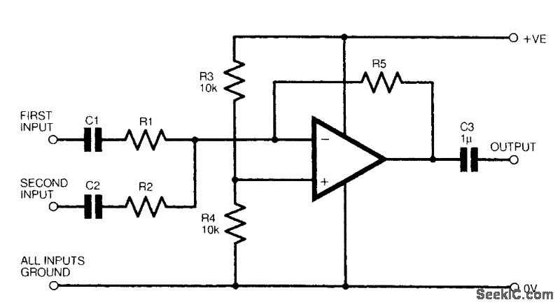
The figure illustrates a fundamental two-channel operational amplifier (op-amp) mixer circuit. The gain for channel 1 is determined by the ratio of resistors R5 to R1, while for channel 2, it is determined by the ratio of R5 to...

AMIS-49200-XTP is a subpackage of AMIS-492X0. For further information, please refer to the description of AMIS-492X0. The datasheet for AMIS-49200-XTP can be downloaded from the link provided below. By ON Semiconductor. The AMIS-49200-XTP is a specialized integrated circuit designed for...

This circuit was developed to create a simple network tester that can be operated by a single individual. Commercial units typically require a second person to monitor the remote LEDs, as the transmitters lack the ability to continuously cycle...

The circuit depicted in Figure 3-150 involves a contactor (KM1) that releases when the system is shut down. The contactor KM2 is energized, allowing a 220V AC power supply to flow through diodes VD1 and VD2, which serve as...

This circuit is designed for children's entertainment and can be installed on bicycles, battery-powered cars, motorcycles, as well as various models, games, and toys. When switch SW1 is positioned as indicated in the circuit diagram, it generates the typical...