
Frequency Divider circuit

The frequency divider circuit utilizes a T-flip flop, which is a type of bistable multivibrator. The T-flip flop toggles its output state on each clock pulse received at its input. In this implementation, the input clock signal is derived from a sine wave source, which is first conditioned to remove the negative half-cycle. This is typically accomplished using a comparator or Schmitt trigger circuit to ensure that the output is a clean square wave.
The IC used, the 4011, is a quad 2-input NAND gate, which can be configured to perform the necessary logic operations for the T-flip flop. The output frequency is half of the input frequency due to the nature of the T-flip flop operation, where each transition of the input clock results in a state change in the output.
The power supply for this circuit is modest, requiring only +5V, making it suitable for low-power applications. The current draw is minimal, allowing for efficient operation in battery-powered devices or low-energy systems. The design is straightforward and can be easily implemented on a breadboard or a PCB for prototyping purposes.
Overall, this frequency divider circuit serves as an essential building block in digital electronics, enabling the manipulation of signal frequencies for various applications, including clock generation and signal processing.This is a classic divider of frequency via two. It is achieved with a classic circuit T-flipFlop, round IC1 [ 4011 ]. In the circuit, the frequency of network, after are limit the negative half-s period of sine wave and transform in square wave, are divided via two. Thus for frequency50 HZ, we will take in the exit pulse of frequency 25 HZ. The supply of circuit it is + 5V and does not need high benefit in current.. 🔗 External reference
Related Circuits

This basic tuned LC amplifier can be used with three output coupling methods: capacitive coupling output, capacitive tapped output, or link-coupled output. The tuned LC amplifier is a fundamental circuit used in various applications, including radio frequency (RF) amplification and...
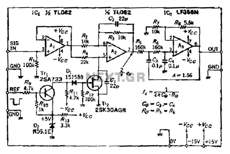
After turning off TT2, the input signal enters through chi Az, where the input resistance is very high and reaches the same potential. The inverting input terminal must also be associated with this movement. Therefore, Trr functions as a...
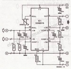
The microphone preamplifier circuit design presented in this schematic utilizes the SSM2015 produced by Precision Monolithics Inc. (PMI), which offers high amplification. The SSM2015 is a low-noise, low-distortion integrated circuit designed specifically for microphone preamplification. It features a differential input...
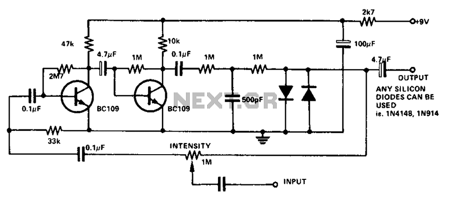
The circuit utilizes a transistor to amplify the input signal. Two diodes are employed to clamp the distorted output, while a 500 pF capacitor filters out high-frequency noise. Under normal conditions, a 1M slide rheostat is used to adjust...
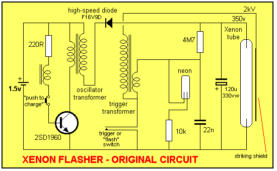
This discussion covers three different Xenon flashing circuits from disposable cameras. From these circuits, unique techniques not found in any theoretical literature will be presented. The first circuit consists of six building blocks. An old disposable flash camera and...
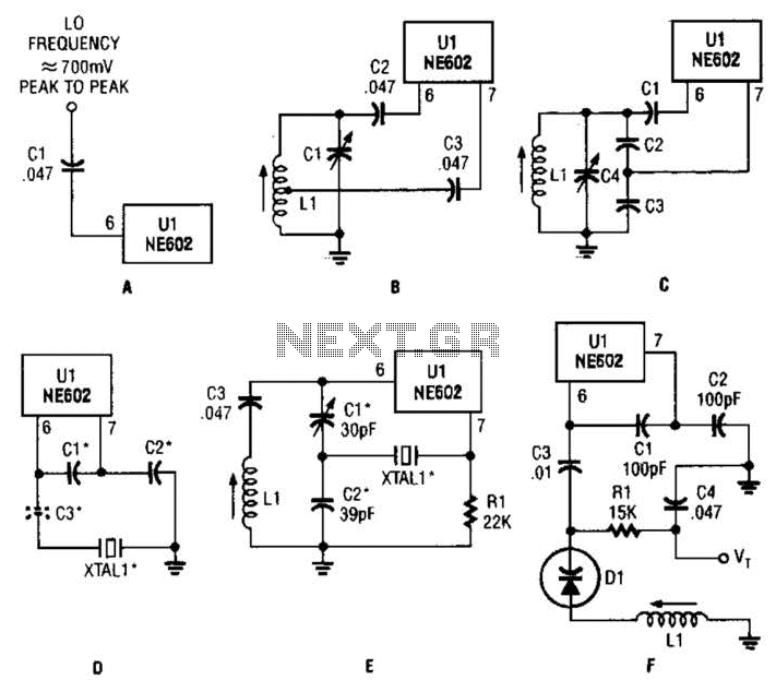
Any standard oscillator, such as a Colpitts or Hartley configuration, can be utilized to generate the local oscillator (LO) frequency required by the NE602. The NE602 is a versatile integrated circuit commonly used in radio frequency applications, particularly in mixer...