
Fuzz Face


The Voltage Feedback (VF) circuit has the properties that it offers the potential for the highest possible gain from any given transistor - good for a distortion device. It also has a very low input impedance, which means that it heavily loads anything trying to drive it. This will be an important point later. Finally, it can't really hard saturate like many other transistor hookups. When driven with a large signal on the base, the collector voltage moves toward the emitter. This lowers the bias voltage through the 100K biasing resistor and steals some of the input signal. Saturation is mushy - again, very good for a musical sounding device.
Was this intentional on the part of the designer? Probably not. It's likely it was a happy accident, as the VF circuit was common in the early days of circuit design to wring more gain from poor transistors.
The voltage swing in the other direction, when the input is trying to turn the first transistor off, is not as constrained as the swing towards saturation. Fuzz Faces naturally tend to bias with only about half a volt on the collector of the first transistor, so there is a lot of room upwards. The input stage will first hit mushy saturation on one polarity of signal and then if driven hard enough, hit cutoff on the other polarity. The Fuzz Face has asymmetrical clipping designed into it!
The second transistor serves a couple of purposes. The base is directly coupled to the collector of the first transistor; the bias current then is largely set by the value of the emitter resistor - in this case a 1K pot. The pot forces the static current through the device to be equal to the first collector voltage minus the base emitter voltage of the second transistor, divided by the 1K resistance. That same current, essentially, flows through the collector resistance of the device, and the voltage across the two collector resistors is equal to the static current times the sum of the resistances. Because the first transistor biases up so close to ground, there is still plenty of room for the second transistor to have some collector-emitter voltage left over for a linear swing.
The gain of the second stage is approximately determined by the ratio of the AC load in the collector to the AC load on the emitter. The AC collector load is just the sum of the collector resistors, and the emitter load to AC is the portion of the 1K pot not "shorted" to ground through the 20uF capacitor. So the gain can vary from a low of about 8 to as high as the transistor's basic internal gain when the pot is maxed out. There is a secondary effect in that the AC gain of the FIRST stage is also set by the AC feedback from that pot through the 100K resistor, so when the control is turned full down, the feedback reduces the first stage's gain most. As the control is turned up more, less AC is fed back to the input, so the effective gain goes up.
As the second stage is driven harder, it can hard clip in cutoff on the same polarity that the first stage clipped softly on, so the clipping begins softly for smaller signals (and gains) and then transitions to hard clipping with harder playing - the thing gets touch sensitivity!
The split collector load resistor of the second transistor acts like a volume pot permanently set to a low value. This is because the power supply is effectively at AC ground because of the low AC impedance of the battery. Incidentally, this is why the Fuzz Face sounds different with different batteries and with the same battery as it gets run down - the impedance of the battery can change the effective value of the smaller resistor by a significant amount.
The circuit design outlined incorporates two NPN transistors configured in a voltage feedback arrangement, which is fundamental for achieving the desired distortion characteristics. The first transistor receives the input signal through a DC blocking capacitor, preventing any DC offset from affecting the input stage. The emitter is grounded, and the collector is connected through a resistor to the power supply. This configuration allows the transistor to amplify the input signal while maintaining a low distortion level.
The second transistor, configured as an emitter follower, ensures that the output signal closely follows the input signal from the first transistor, albeit with a slight reduction due to the base-emitter voltage drop. The feedback mechanism established via the 100K resistor allows dynamic adjustment of the gain based on the output voltage of the first transistor, which is critical for achieving the desired tonal characteristics.
The gain structure of the circuit is determined not only by the resistor values but also by the interaction between the two stages. The variable resistor (1K pot) in the emitter circuit of the second transistor allows for fine-tuning of the gain, providing versatility in the distortion characteristics. This tunability is further enhanced by the feedback loop from the second transistor to the first, allowing for a range of gain settings depending on the position of the control.
Overall, this circuit exemplifies a simple yet effective approach to distortion generation, utilizing basic components to create a rich and dynamic sound suitable for various musical applications. The design's sensitivity to input dynamics and the interaction between the two transistors contribute to its unique tonal qualities, making it a popular choice among musicians seeking distinctive fuzz effects.This is simple almost beyond belief for distortion devices. Two transistors, four resistors, three capacitors, and two controls make all that tone. The first transistor is set up with the simplest of arrangements - input through a DC blocking capacitor directly to the base, emitter grounded, and a single collector resistor; the driven load is a second transistor base, directly coupled. For DC purposes, the second transistor acts as an emitter follower. The voltage at it's emitter must follow the first transistor's collector, although it is lower by the amount of the base emitter drop of the second transistor.
To the first transistor, that means that the 100K resistor from the emitter of the second transistor to the first transistor's base is effectively a feedback resistor, passing a current proportional to the first transistor's collector voltage to the first transistor's base. This arrangement is called the "voltage feedback biasing" circuit, and some of the Fuzz Face's unique properties stem from this. The Voltage Feedback (VF) circuit has the properties that it offers the potential for the highest possible gain from any given transistor - good for a distortion device.
It also has a very low input impedance, which means that it heavily loads anything trying to drive it. This will be an important point later. Finally, it can't really hard saturate like many other transistor hookups. When driven with a large signal on the base, the collector voltage moves toward the emitter. This lowers the bias voltage through the 100K biasing resistor, and steals some of the input signal. Saturation is mushy - again, very good for a musical sounding device. Was this intentional on the part of the designer? Probably not. It's likely it was a happy accident, as the VF circuit was common in the early days of circuit design to wring more gain from poor transistors.
The voltage swing in the other direction, when the input is trying to turn the first transistor off, is not as constrained as the swing towards saturation. Fuzz Faces naturally tend to bias with only about half a volt on the collector of the first transistor, so there is a lot of room upwards.
The input stage will first hit mushy saturation on one polarity of signal and then if driven hard enough, hit cutoff on the other polarity. The Fuzz Face has asymetrical clipping designed into it! The second transistor serves a couple of purposes. The base is directly coupled to the collector of the first transistor; the bias current then is largely set by the value of the emitter resistor - in this case a 1K pot.
The pot forces the static current through the device to be equal to the first collector voltage minus the base emitter voltage of the second transistor, divided by the 1K resistance. That same current, essentially, flows through the collector resistance of the device, and the voltage across the two collector resistors is equal to the static current times the sum of the resistances.
Because the first transistor biases up so close to ground, there is still plenty of room for the second transistor to have some collector-emitter voltage left over for a linear swing. The gain of the second stage is approximately determined by the ratio of the AC load in the collector to the AC load on the emitter.
The AC collector load is just the sum of the collector resistors, and the emitter load to AC is the portion of the 1K pot not "shorted" to ground through the 20uF capacitor. So the gain can vary from a low of about 8 to as high as the transistor's basic internal gain when the pot is maxxed out.
There is a secondary effect in that the AC gain of the FIRST stage is also set by the AC feedback from that pot through the 100K resistor, so when the control is turned full down, the feedback reduces the first stage's gain most. As the control is turned up more, less AC is fed back to the input, so the effective gain goes up. As the second stage is driven harder, it can hard clip in cutoff on the same polarity that the first stage clipped softly on, so the clipping begins softly for smaller signals (and gains) and then transistions to hard clipping with harder playing - the thing gets touch sensitivity!
The split collector load resistor of the second transistor acts like a volume pot permanently set to a low value. This is because the power supply is effectively at AC ground because of the low AC impedance of the battery.
Incidentally, this is why the FF sounds different with different batteries and with the same battery as it gets run down - the impedance of the battery can change the effective value of the smaller resistor by an significant amount. 🔗 External reference
Related Circuits
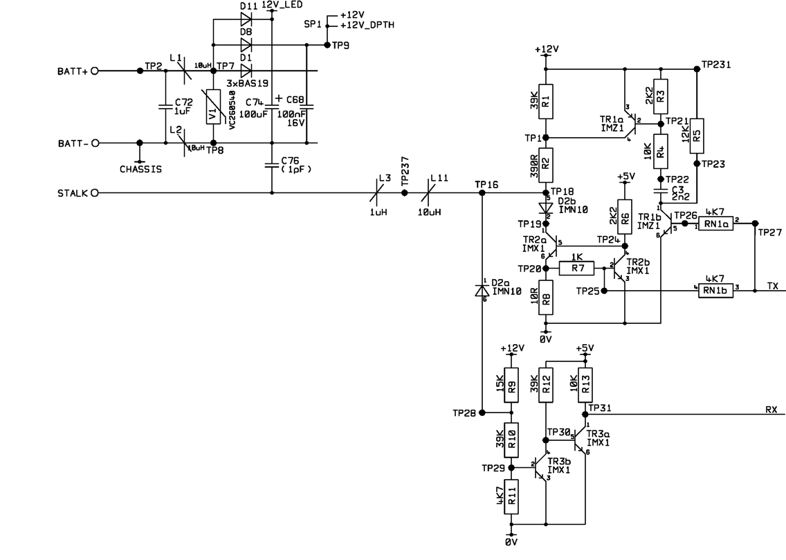
A project involves using a PIC microcontroller to communicate with the Raymarine SeaTalk bus. The schematic diagram for a Raymarine instrument shows a logic chip connected to the TX and RX connections on the right side, while the SeaTalk...
A method for measuring static electricity for a science project was sought. An old copy of "Getting Started in Electronics" by Forrest M. Mims III was referenced for guidance. To create a static electricity measurement circuit, a simple design can...
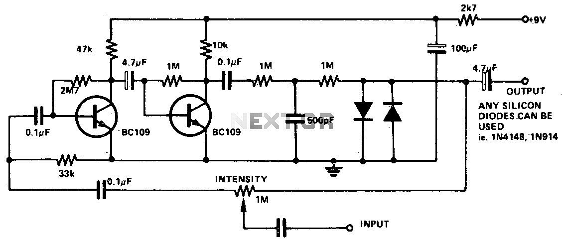
The input signal is amplified by the transistors. The distorted output is then clipped by the two diodes, and the high-frequency noise is filtered from the circuit via the 500 pF capacitor. The 1 M potentiometer adjusts the intensity...

The circuit depicted in the schematic utilizes zero-drift operational amplifiers (LTC1250 and LTC1050) along with a precision instrumentation switched capacitor block (LTC1043). This design achieves exceptional DC accuracy down to microvolt levels. The choice of this method over a...
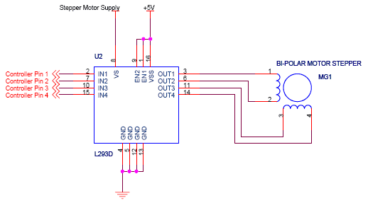
The circuit features four pins labeled "Controller pin 1," "Controller pin 2," "Controller pin 3," and "Controller pin 4," which are responsible for controlling the motion and direction of the stepper motor based on the step sequence programmed into...

This project demonstrates the interfacing and operation of the Nokia 3310 LCD using the PIC16F628 microcontroller. The programming is executed in Hi-Tech C, with the character table incorporated within the source code. The Nokia LCD features a resolution of...