
High frequency analog switch

The commutator circuit is designed to optimize the performance of the PN4091 analog switch, which is critical in applications requiring efficient signal routing and switching. The low impedance gate drive ensures that the switch can be turned on and off rapidly, which is essential for high-frequency operations.
In the on state, the circuit provides high AC impedance, which minimizes power loss and allows for better signal integrity. This high impedance state is crucial for maintaining the quality of the signal being switched, particularly in high-speed applications where signal degradation can lead to performance issues.
Conversely, during the off state, the circuit presents a low AC impedance to the PN4091. This characteristic is vital for quickly discharging any residual charge from the gate of the switch, ensuring that it turns off efficiently and without delay. The low impedance allows for faster recovery times, enhancing the overall switching speed and responsiveness of the circuit.
The careful design of the commutator circuit, including the selection of components and their arrangement, plays a significant role in achieving these impedance characteristics. Capacitors, resistors, and possibly inductive elements are strategically utilized to create the desired impedance profiles. The circuit may also incorporate feedback mechanisms to further refine the gate drive characteristics, ensuring that the PN4091 operates effectively across a range of frequencies and signal conditions.
Overall, the commutator circuit is a critical component in systems utilizing the PN4091 analog switch, enabling high-performance operation with minimal signal degradation and rapid switching capabilities.Commutator circuit provides low impedance gate drive to the PN4091 analog switch for both on and off drive conditions This circuit also approaches the ideal gate drive conditions for high frequency signal handling by providing a low ac impedance for off drive and high ac impedance for on drive to the PN4091.
Related Circuits
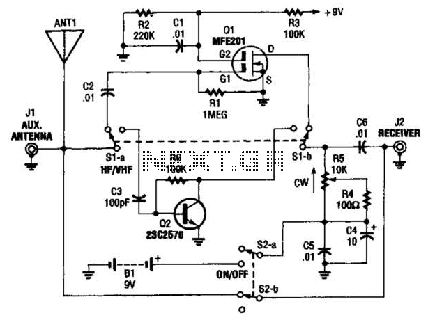
The AA-7 active antenna consists of two active components: Q1 (an MFE201 N-channel dual-gate FET) and Q2 (a 2SC2570 VHF silicon transistor), which form the foundation for two independent, switchable RF preamplifiers. The AA-7 active antenna is designed to enhance...

Superheterodyne receivers have been mass-produced since around 1924, but for reasons of cost did not become successful until the 1930s. Superheterodyne receivers represent a pivotal advancement in radio technology, characterized by their ability to convert high-frequency signals into lower...
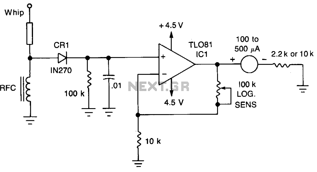
A TL081 operational amplifier (IC1) is utilized to enhance sensitivity. The RF signal is detected by CR1 and subsequently amplified by IC1. Full-scale sensitivity is adjusted using a 100-ohm potentiometer. The circuit employs a TL081 operational amplifier, known for its...

CRTGND is not equivalent to GND; CRTGND connects to the MOSFET drain or Schottky diode. A disadvantage of this circuit is the voltage drop when powered from the USB side due to the diode. The USB voltage can fluctuate...
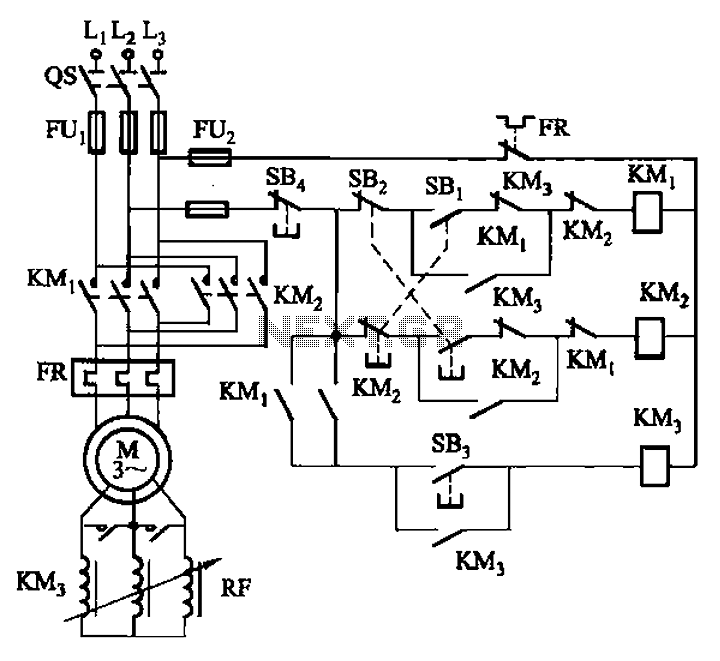
The circuit illustrated in Figure 3-166 employs a button control mechanism. To initiate forward motion, the user presses button SB1, which activates the motor rotor through a frequency-sensitive rheostat (RF). As the motor speed approaches its rated speed, a...
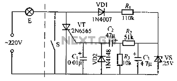
A delay circuit using an improved quenching lamp pull switch is described, focusing on its performance and the delay function in lighting control. The circuit exhibits a high degree of stability and reliability. When switch S is closed, the...