
Pull switch lights delay circuit 2

The described circuit utilizes a quenching lamp pull switch mechanism to create a controlled delay in lighting applications. The operational principle relies on the charging and discharging characteristics of the capacitor (C) in conjunction with the thyristor (VT) and associated components. Initially, when switch S is closed, the circuit remains inactive, preventing any current flow through the light bulb connected to E. Upon opening switch S, the AC voltage is applied to the circuit, allowing the diode (VD1) to rectify the input voltage, while the capacitor (C) begins to charge.
The design incorporates a 25V voltage regulator (VS) which ensures that the voltage across the capacitor does not exceed this limit, thus providing stable operation. The thyristor (VT) is triggered by the voltage across the capacitor via the resistor (R). Once triggered, the thyristor allows current to flow through the AC bulb, producing a dim light output. The gradual charging of the capacitor results in a delay before the thyristor is turned off, which occurs when the capacitor reaches full charge and the AC voltage crosses zero.
The circuit's ability to control the delay time is achieved by modifying the capacitance of capacitor C. A larger capacitance will increase the charge time, thereby extending the delay period, while a smaller capacitance will reduce it. The resistor R and variable resistor VR2 play crucial roles in the discharge process, allowing the stored charge in the capacitor to be released efficiently, preparing the circuit for the next activation cycle. Overall, this delay circuit is suitable for applications requiring precise timing in lighting control, ensuring both reliability and stability in operation.A delay by the improved quenching lamp pull switch, its performance and the example described delay lights care line switches, but the work of a high degree of stability and go od reliability. When S is closed, lights, electronic circuits on the right does not work. Ge lights, s open, 220V AC electric bulb through E, a half-wave rectifier diode VD1, foot t buck limit the flow of C. Charged by the charging time constant dry small, G soon full charge. c, in parallel across a 25V regulator vs. So C, both ends of the business flow voltage is clamped at about 25V. This fork 25V DC voltage through R, VT to the cathode gate capacitance [1. Yun electricity, this allows the electric current is triggered thyristor VT iU flows, thus opening VT is triggered.
AC bulb half crossing through, so see the light bulb E send weak lighting. After about tens of seconds, c charge is full, VT lost trigger current, when the AC zero crossing that is turned off, the light goes off. Turn on the lights again, s closed, lights. Then s voltage drop across zero, C, and stored charge by R. vr2 venting, the discharge time constant is small, electric charge is done and soon put out for the next spider ready for the delay circuit delay lights depends on the length of time the main calyx (j charging electric call the time constant of the road, using data illustrating the delay time is about 40s.
to extend or shrink when cerium peaks J, canthus can increase or decrease the capacitance C. capacity.
Related Circuits
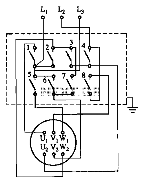
The circuit illustrated in Figure 3-36 includes the starter contact closure detailed in Table 3-1. In the figure, U1, V1, W1, and U2, V2, W2 represent the first three-phase stator windings of the motor terminals. The circuit depicted in Figure...
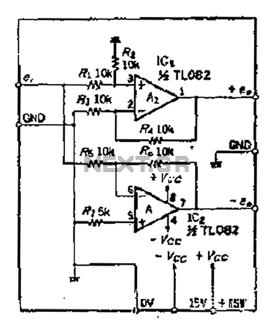
A balanced output is often associated with the positive phase amplifier output terminal of an operational amplifier, which is typically viewed as the inverting amplifier circuit. However, the reversed phase output can lead to a loss of balance in...
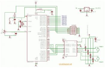
The complete electrical circuit diagram of a line follower robot is based on the ATmega16 microcontroller. This robot consists of three primary modules: the sensor module, the microcontroller module, and the DC motor module. A comprehensive tutorial, including circuit...
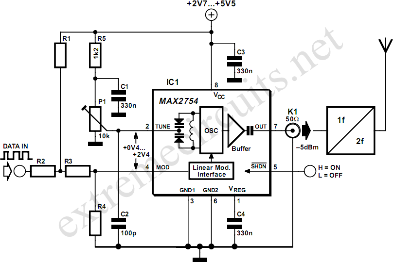
High-frequency voltage-controlled oscillators (VCOs) are challenging to construct, which is why Maxim has developed the integrated 1.2 GHz oscillator, the MAX2754. The center frequency is adjustable via the TUNE input, while a linear modulation input allows for frequency modulation....
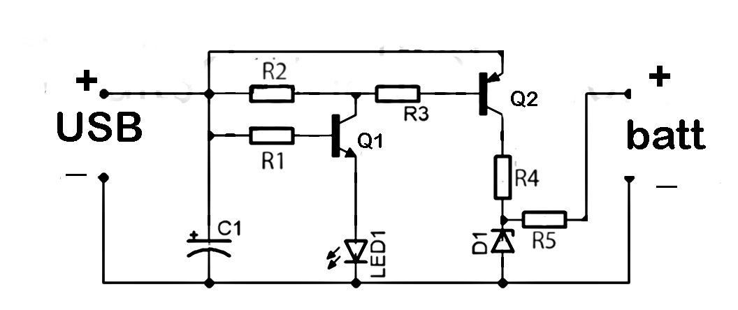
This document discusses the series used in USB connections for charging batteries. The output voltage ranges from 4.7 volts to 5 volts DC, which is suitable for charging mobile phones and other battery types. The circuit described enhances the...
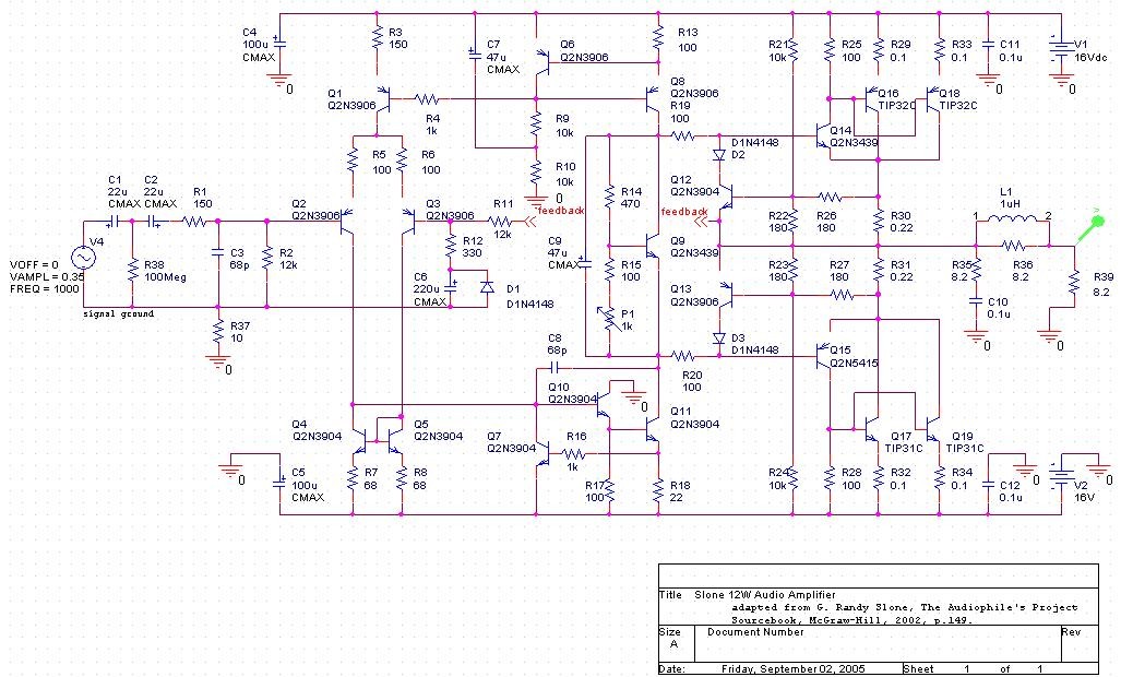
The project involves developing a 12W power amplifier circuit into a fully assembled hard-wired unit. This will require a design cycle and development sequence that includes analysis, simulation, printed circuit board (PCB) layout, board population, hard soldering, and testing....