
High voltage power supply and boost for the BST capacitor DAC provides a tuning signal circuit diagram

The circuit design begins with the ADP1613 boost converter, which is responsible for stepping up the input voltage to the required high voltage levels necessary for the BST capacitors. The output voltage can be adjusted to meet the specific requirements of the application, ensuring that the BST capacitors operate effectively under varying conditions. The AD5504 DAC plays a crucial role in generating the precise voltage levels required for tuning the BST capacitors. By converting digital signals into analog voltage levels, the DAC allows for fine control over the capacitance, enabling precise adjustments that are essential for tuning applications.
The integration of these components into a compact circuit layout is critical, as it minimizes the overall footprint while maintaining performance. The small size of the circuit board, at just 43 mm², allows for easy integration into various electronic systems, including portable devices where space is a premium. Additionally, the use of standard packages like the MSOP and TSSOP facilitates manufacturing and assembly processes, contributing to cost-effectiveness.
The potential applications of this circuit extend beyond just tuning antenna arrays and filters. The boost converter's capability to provide high voltage also makes it suitable for LED driving applications, where high currents and voltages are needed to drive light-emitting diodes efficiently. Furthermore, in optical communication systems, this circuit can serve as a bias voltage source and a receiver, enhancing the versatility of the design.
In summary, the circuit illustrated in Figure 1 not only meets the specific requirements for tuning BST capacitors but also presents a flexible solution for various high-voltage applications in modern electronic systems. Its compact design, combined with the functionality of the ADP1613 and AD5504, positions it as a valuable component in the development of advanced electronic devices. As shown in FIG. 1 circuit generates high voltage signal for controlling BST (barium strontium titanate) capacitors capacitance. Simply applying a voltage of V and 3V to the co rrect terminals, it can change the BST capacitance. Thus, changing the dielectric thickness, thus changing the capacitance. BST commonly used for tuning antenna arrays and tunable filters. Especially for these tuning applications have obvious advantages, for example, the compensation component tolerance errors, fine tuning or filter cutoff frequency for adjustable antenna impedance matching network. Figure 1. The boost power supply and high-voltage DAC provides a tuning signal BST capacitor (simplified schematic: All Connections Not Shown) Such applications require a convenient, compact, low-cost circuit to generate the high voltage power supply, only for this function to add a separate power supply is usually not practical.
Figure 1 circuit ADP1613 boost converter and AD5504 30 V/6V DAC will meet the above requirements. Boost regulator circuit board of a total area of only 43 mm2. ADP1613 is available in 8-pin MSOP package, AD5504 16-pin TSSOP package. Boosting circuit can also be used for LED driver applications, a bias voltage and providing a receiver in optical communication systems.
Related Circuits
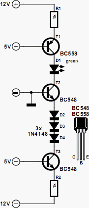
A circuit for monitoring supply voltages of ±5 V and ±12 V can be constructed as shown in the diagram. It is significantly simpler than the typical monitors that utilize comparators and AND gates. The circuit is not designed...
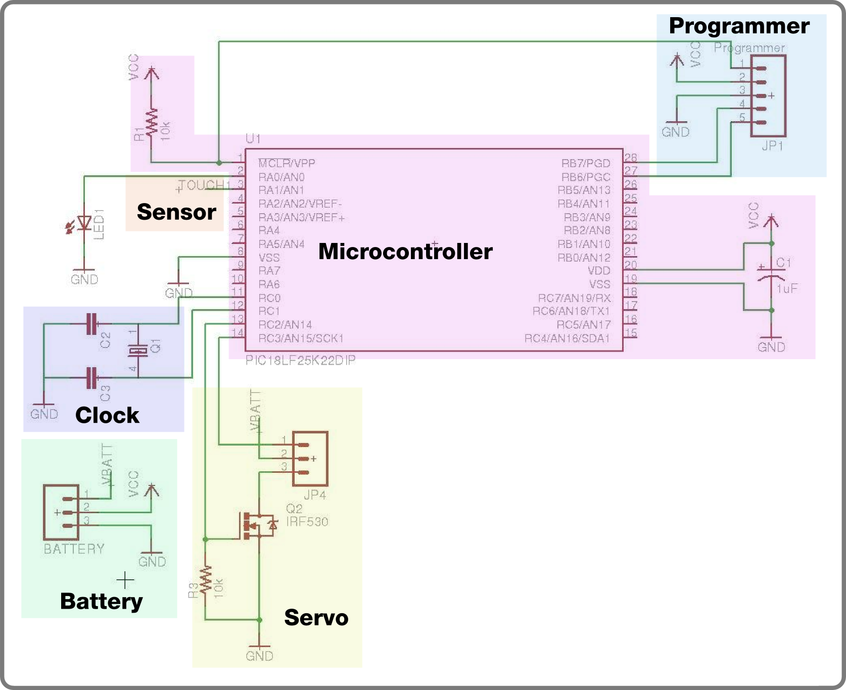
For the second build in the Make It Last Build Series, a robotic plant is being constructed. This week focuses on assembling the control circuit, which will be used in future weeks to animate the plant. The basic circuit...
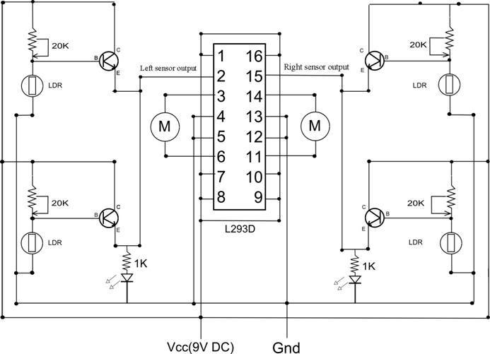
This tutorial outlines the construction of a simple and low-cost robot primarily designed as a line follower. It can also function as a photovore, photophobe, and obstacle avoider, all for less than $40. Notably, the robot does not utilize...
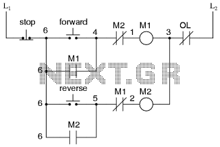
This is the power diagram for motor forward and reverse operation. To change the motor direction, one polarity must be altered, for example, changing R to S. For detailed information, please refer to the following. The described power diagram illustrates...
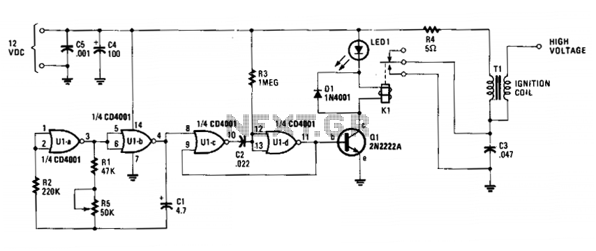
The circuit is fundamentally an auto ignition coil paired with a set of points that perform a similar function. It employs a pulsing circuit constructed from a single CMOS NOR integrated circuit (U1) to open and close relay contacts,...
Numbered components are designated for PC-board layout purposes. C5 and C8 are disc ceramic capacitors. C6 and C7 are tantalum or electrolytic capacitors. R1, R2, and R3 are 1/4 W carbon composition resistors. Silver-mica capacitors may be substituted for...