
HS-3182 ARINC 429 Bus Interface Line Driver Circuit

The HS-3182 differential line driver is engineered to facilitate reliable data transmission in environments adhering to ARINC 429 specifications, commonly used in avionics systems. The dielectrically isolated design ensures that the driver maintains signal integrity while minimizing noise and interference. The integration of TTL and CMOS compatibility allows for seamless interfacing with a variety of digital systems, enhancing versatility in application.
The inclusion of CLOCK and SYNC inputs, which are ANDed with the DATA signals, provides flexibility in synchronizing data transmission, thereby improving the overall performance of the communication system. The requirement for three distinct power supplies (+15V, -15V, and 5V) is indicative of the device's robust design, enabling it to handle varying voltage levels essential for differential signaling.
The programmable output voltage swing, determined by VREF, allows for customization according to specific application needs. This feature is particularly beneficial in systems requiring precise voltage levels for optimal performance. The capability to use external capacitors to adjust rise and fall times provides additional control over signal timing, which is critical in high-speed data applications.
The HS-3182's output protection mechanisms safeguard against overvoltage and short circuit conditions, ensuring reliability and longevity in operation. Furthermore, the specified operating temperature ranges of -55 °C to +125 °C and -40 °C to +85 °C indicate the device's suitability for harsh environmental conditions typically encountered in aerospace applications. This comprehensive set of features positions the HS-3182 as a vital component in advanced communication systems, ensuring effective and efficient data transmission.The HS-3182 is a monolithic dielectrically isolated bipolar differential line driver designed to meet the specifications of ARINC 429. This Device is intended to be used with a companion chip, HS-3282 CMOS ARINC Bus Interface Circuit, which provides the data formatting and processor interface function.
All logic inputs are TTL and CMOS compatible. In addition to the DATA (A) and DATA (B) inputs, there are also inputs for CLOCK and SYNC signals which are AND`d with the DATA inputs. This feature enhances system performance and allows the HS-3182 to be used with devices other than the HS-3182.
Three power supplies are necessary to operate the HS-3182: +V = +15V ±10%, -V = -15V ±10%, and V1 = 5V ±5%. VREF is used to program the differential output voltage swing such that VOUT (DIFF) = ±2VREF. Typically, VREF = V1 = 5V ±5%, but a separate power supply may be used for VREF which should not exceed 6V.
The driver output impedance is 75 ±20% at +25 °C. Driver output rise and fall times are independently programmed through the use of two external capacitors connected to the CA and CB inputs. Typical capacitor values are CA = CB = 75pF for high-speed operation (100kBPS), and CA = CB = 300pF for low-speed operation (12kBPS to 14.
5kBPS). The outputs are protected against overvoltage and short circuit as shown in the Block Diagram. The HS-3182 is designed to operate over an ambient temperature range of -55 °C to +125 °C, or -40 °C to +85 °C. 🔗 External reference
Related Circuits
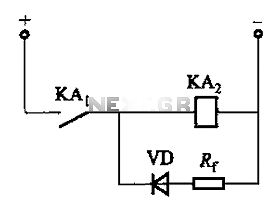
The circuit depicted in Figure 6-24 includes a relay coil with both ends connected in parallel to a resistor (Rf) or an auxiliary diode (VD). This configuration is intended to enhance power after a short circuit occurs in the...

This circuit generates sine and square wave signals with frequencies ranging from below 20 Hz to above 20 kHz. The advantage of this circuit diagram is that the output frequency can be adjusted by varying the variable resistor R6. The...
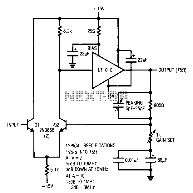
Q1 and Q2 create a differential stage that transitions into the LT1010. The capacitively terminated feedback divider provides a gain of 1, while permitting AC gains of up to 10. With a 20-ohm bias resistor, the circuit outputs 1...
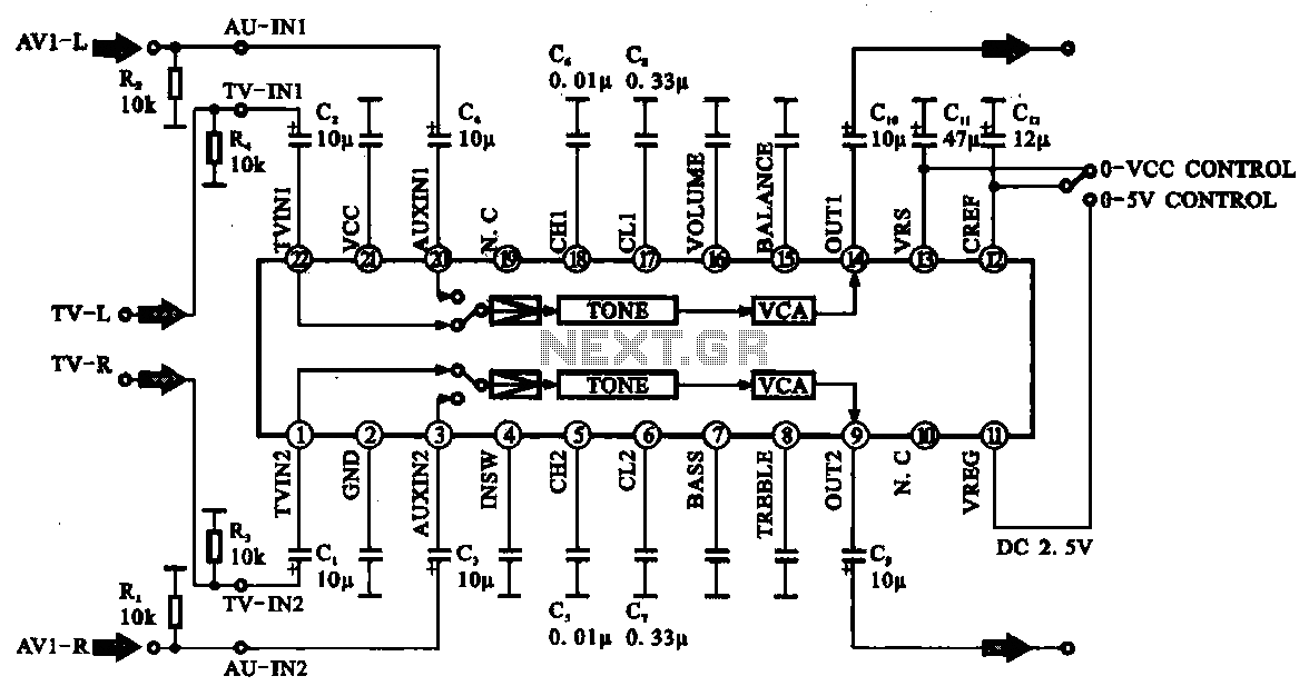
Audio signal control circuit. It illustrates a typical audio signal control circuit where two audio signals enter the integrated circuit through switching and tone controls (treble and bass), subsequently adjusting the output sent to the audio power amplifier. The audio...
T-121 temperature sensor electronic thermometer circuit diagram shown below The T-121 temperature sensor circuit is designed to measure and display temperature readings accurately. The circuit typically consists of a temperature sensor, such as the T-121, which converts temperature variations into...
The original smoke alarm circuit has several issues that have disappointed hobbyists and students. Instead of attempting to fix these problems, an update has been created using the well-known LM741 operational amplifier. This new design is simpler, more conventional,...