
Human reaction speed test circuit

The human reaction speed test circuit is designed to measure the response time of an individual by utilizing a series of digital components that work in conjunction. The core of the circuit is the IC1, an 8-bit register that stores the timing data. The clock pulse, generated by the multivibrator circuit, operates at a frequency that allows for precise timing control, set at approximately 50 milliseconds. This timing is critical for accurately capturing the reaction times of participants.
The boot delay circuit, represented by D1, ensures that the system is initialized correctly before the test begins. When the output of D1 is high ("1"), the IC1 registers a series of high values in rapid succession. This setup remains active for a predetermined duration of 3 to 4 seconds, during which the participant is expected to respond to the test signal indicated by VD1. The transition of D1 to low ("0") signifies the start of the reaction test.
Once the test signal is activated, the 8-bit storage unit begins resetting its values from high ("1") to low ("0") under the clock pulse influence. The participant must then press the stop button (S1) to halt the test. The RS flip-flop, formed by D3 and D4, plays a crucial role in maintaining the state of the circuit, ensuring that the output signal to the NAND gates (D25 and D26) stops the vibration mechanism, thus concluding the timing sequence.
The results of the test are communicated through a series of drive circuits (D13 to D16 and D21 to D24), which control the activation of light-emitting diodes. These LEDs provide a visual representation of the participant's reaction time, making it easy to assess performance. Additionally, the inclusion of D2 serves a protective function, preventing the stop button from being registered until the test signal is fully operational, thereby ensuring the integrity of the test results. Overall, this circuit efficiently combines digital logic components to create an interactive and effective human reaction speed testing device.Human reaction speed test circuit as shown in FIG. NAND gate D25, D26 and other components multivibrator output clock pulse period is about 50ms. IC1 composition 8 right register, D1 composed of boot delay circuit output signal as its serial input data. Just machines, since D1 output is "1" in the clock pulses, IC1 8-bit storage unit quickly all "1"; after 3s ~ 4s, D1 output to "0", the test signal VD1 light, while, IC1 8-bit storage unit under the clock pulses from left to right to "0" until the person being tested press the stop button S1, the D3, RS flip-flop D4 composed of "0" so that D25, D26 stop vibration, IC1 is on hold, the result through the drive circuit D13 ~ D16, D21 ~ D24 drive the light emitting diode display. D2s role is to make the stop button S1 tests only after the bright lights VD1 acts invalid press ahead.
Related Circuits

A single-phase rectifier DC welding power load from the road circuit is presented. The contactor KM utilizes a CJ20-40A model rated for 220V. An adjustment potentiometer RP is employed to ensure proper arcing, while the relay KA2 is designed...
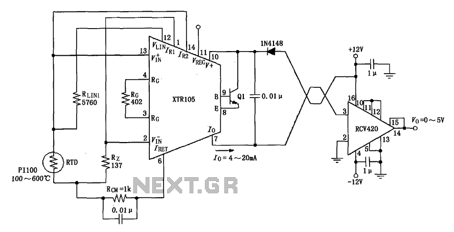
The circuit utilizes a Pt100 type resistance temperature detector (RTD). It operates within a temperature range of 100 to 600 °C, where the XTR105 outputs a current of 4 to 20 mA, and the RCV420 provides an output voltage...
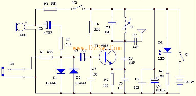
C4 and L form a resonator, where the resonant frequency corresponds to the FM transmitting power of the microphone. According to the component parameters in the diagram, the transmission frequency can range from 88 to 108 MHz. The frequency...
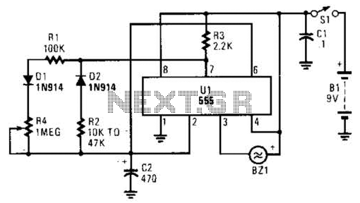
This timer circuit utilizes a 555 IC timer in conjunction with three 74LS193 counters to control an LED display. The circuit is activated by one individual who turns on the piezo buzzer BZ1 through Q1, simultaneously starting the timer....
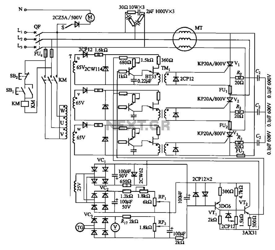
The circuit depicted in Figure 3-181 comprises three thyristors, labeled V1 to V3. The trigger circuit utilizes a single-junction transistor relaxation oscillator. The speed control circuit incorporates negative feedback. A master adjust potentiometer, designated as RPi, is used to...

This circuit provides protection for telephones, EPABX systems, telephone modems, and similar devices against lightning discharges and line voltage spikes. It incorporates a safety capacitor and gas discharge components. The circuit employs a safety capacitor to filter out high-frequency noise...