
interfacing to microprocessor
The parallel interface functions as a robust communication method for transferring multiple bits of data concurrently, making it particularly advantageous in applications requiring quick and efficient data transfer. Each wire in the parallel interface corresponds to a bit in the data word, allowing for simultaneous transmission of multiple signals. This configuration is beneficial in scenarios where rapid state changes are required, such as in control systems for motors or sensors.
The DAC plays a critical role in converting digital signals into analog form, which is essential for interfacing with analog devices. The operational amplifier in conjunction with the DAC ensures that the current output is transformed into a usable voltage level. The precision of the conversion is directly linked to the resolution of the DAC, which determines how finely the output can be adjusted. As applications demand higher fidelity and finer control, utilizing multiple DACs in tandem can enhance performance by increasing the resolution and range of output voltages.
Similarly, the ADC serves an equally important function in converting analog signals back into digital format, enabling digital processing of real-world signals. The complexity of the ADC operation reflects the need for precise timing and sampling to ensure accurate representation of the input voltage. The relationship between the analog input and the digital output is crucial for applications such as data acquisition systems, where accurate measurements are paramount.
Overall, the integration of DACs and ADCs with parallel interfaces provides a comprehensive solution for interfacing digital systems with the analog world, facilitating a wide range of applications in electronics and control systems.The parallel interface transfers data 8 bits (or more) at the same time, using eight separate wires. It is essentially an extension of the data bus into the outside world. The parallel interface is ideal for inputting or outputting data from devices that are either on or off. For example, a single limit switch uses only one input bit, and an on-of f signal to a motor requires only one output bit. These 1-bit signals are called logic variables, and eight such signals can be provided from a single (8-bit) port. This concept In other applications, the controller may use a parallel interface to connect to an analog device ”for example, driving a variable-speed DC motor.
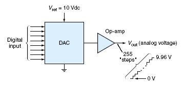
In such a case, the binary output of the controller must first be converted into an analog voltage before it can drive the motor. This operation is performed by a special circuit called a digital-toanalog converter. The digital-to-analog converter (DAC) is a circuit that converts a digital word into an analog voltage.
It is not within the scope of this text to describe the internal workings of the DAC, but a general understanding of the operating parameters is appropriate. Figure 2. 5 shows the block diagram of a typical 8-bit DAC. The input is an 8-bit digital word. The output is a current that is proportional to the binary input value and must be converted to a voltage with an op-amp.
A stable reference voltage (Vref) must be supplied to the DAC. This voltage defines the maximum analog voltage ”that is, for a digital input of 11111111, Vout is essentially Vref. If the input is 00000000, the Vout will be 0 Vdc. For all values in between, the output voltage is a linear percentage of Vref. Specifically, the output voltage for any digital input (for the 8-bit DAC) is An important consideration of digital-to-analog conversion is resolution.
The resolution of a DAC is the worst case error that is introduced when converting between digital and analog. This error occurs because digital words can only represent discrete values, as indicated by the stair-step diagram in Figure 5.
For example, the maximum value of an 8-bit number is 255 decimal, which means there are 255 possible steps of the output voltage. The difference between steps is the value of the least significant bit (LSB). Because the smallest increment is one step, the resolution (for 8-bit data) is 1 part in 255, or 0. 39%. This resolution is adequate for many applications, but if more is needed, two (or more) 8-bit ports can be used together.
Two ports provide 16 bits of data. The maximum decimal value of 16 bits is 65, 535. Being able to divide an analog Figure 6 shows a data sheet for an 8-bit DAC (DAC0808). This device comes as a 16-pin DIP (dual in-line package) and uses an external op-amp (such as the LF 351), two resistors, and a capacitor to complete the circuit. It requires plus and minus powersupply voltages. The time to complete a conversion is a fast 150 ns (nanoseconds). (The An analog-to-digital converter (ADC) is a circuit that converts an analog voltage into a digital word.
A typical ADC consists of a single IC with a few support components. Analog-to-digital conversion is a more complicated process (than for the DAC), and the hardware requires some conversion time, which is typically in the microsecond range. The conversion time required depends on the type of ADC, the applied clock frequency, and the number of bits being converted.
Figure 2. 7 shows a block diagram for an 8-bit ADC. The input Vin can be any voltage between 0 V and Vref. When Vin is 0 Vdc, the output is 00000000; when Vin is Vref, the output is 11111111 (255 decimal). To start the conversion process, a start-conversion pulse is sent to the ADC. The ADC then samples the analog input and converts it to binary. When completed, the ADC activates Figure 8 shows a data sheet for an 8-bit ADC (ADC0804). Packaged as a 20-pin DIP, this device can operate on a single 5-Vdc 🔗 External reference
Related Circuits
The I2C PIC Interfacing Tutorial circuit is relatively straightforward; however, it requires careful verification to ensure that all connections are correct before initial operation. The primary components utilized in this circuit include the PIC18F452 microcontroller, the 24LC02B EEPROM, and...
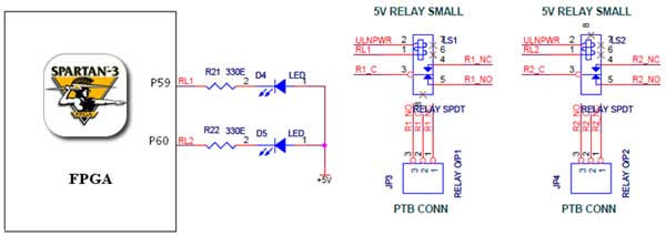
The Spartan-3 board features external 5V relay interfacing, as depicted in the accompanying figure. The ULN2803 is utilized as a driver for the FPGA I/O lines, with the driver outputs connected to the relay modules. A PTB connector is...
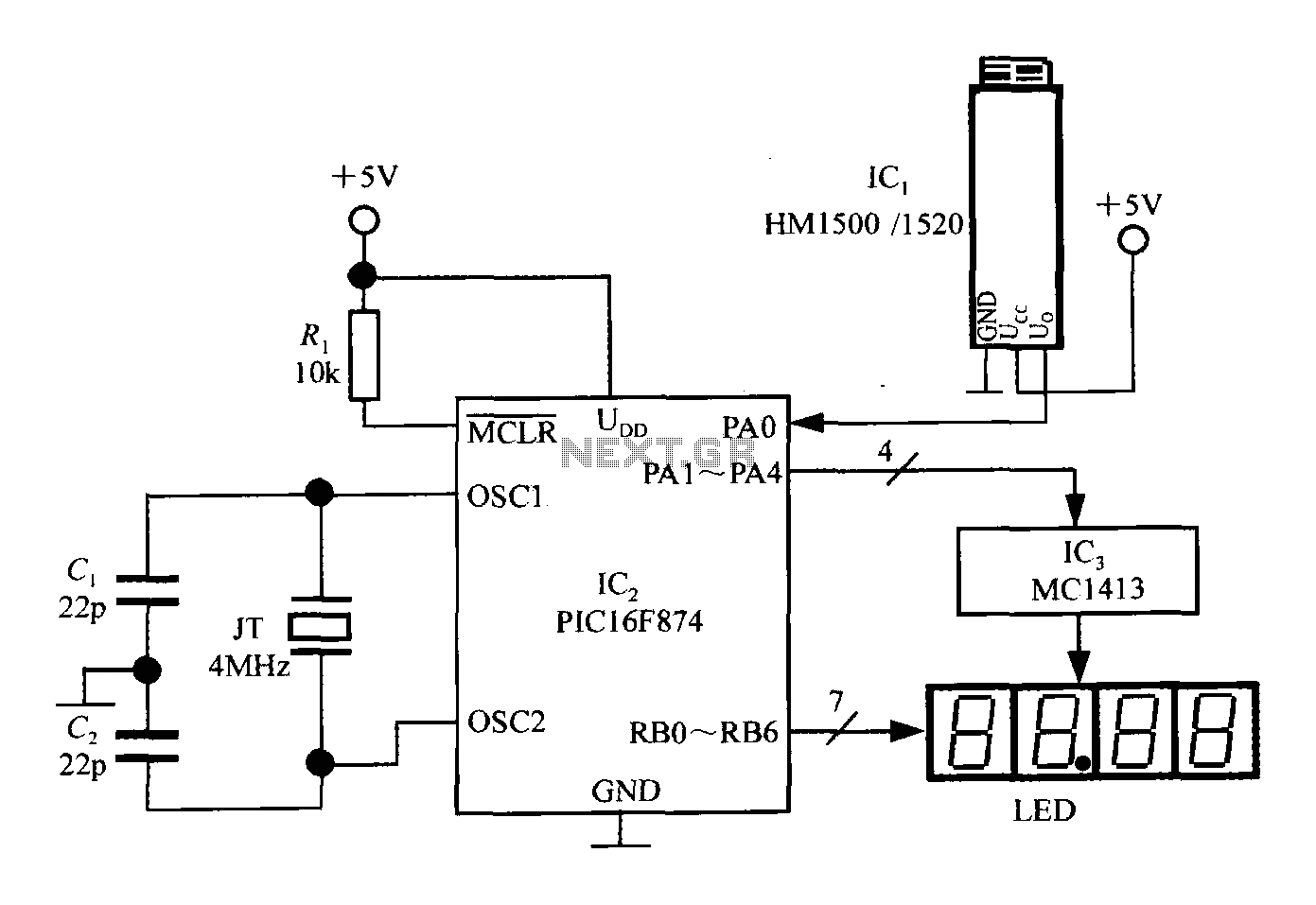
An intelligent humidity meter circuit utilizing the HM1500/1520 humidity sensor and a microcontroller configuration. The circuit operates on a +5V power supply and incorporates four common cathode LED digital displays. It employs three integrated circuits: IC1 is the HM1500/1520...
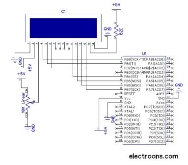
The RW line is the "Read/Write" control line. When RW is low (0), the information on the data bus is being written to the LCD. When RW is high (1), the program is effectively querying (or reading) the LCD....

The LCD does not effectively assist in programming due to the absence of a debugging program. It is necessary to display the results of calculations, the contents of variables, or other debugging information on the LCD to understand the...
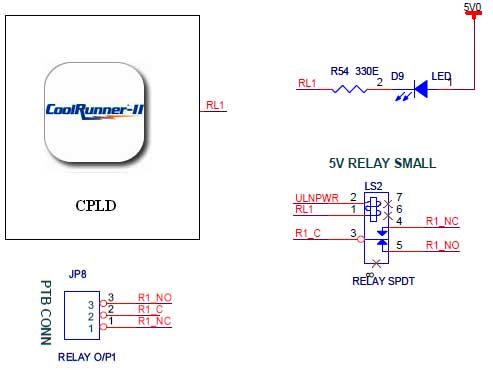
The CoolRunner-II board features external 5V relay interfacing, as indicated in the accompanying figure. The ULN2803 is utilized as a driver for the CPLD I/O lines, with the driver outputs connected to the relay modules. A PTB connector is...