
Inverted 555 Timer Circuit

The inverted 555 timer circuit is designed to overcome the limitations of the standard 555 timer, particularly regarding duty cycle and output polarity. In typical applications, the 555 timer can only achieve duty cycles equal to or greater than 50%, which restricts its versatility in various timing applications. The inverted configuration allows for duty cycles less than 50%, thus expanding the timer's functionality.
The use of the 2N3904 transistor in the first circuit illustrates a common approach for low-voltage applications. However, as the supply voltage (Vcc) increases beyond 9V, the base-emitter junction's zener effect becomes a critical consideration. This behavior can lead to operational instability, necessitating modifications such as the addition of D1 in the second circuit to increase the VEBO rating, thereby extending the operational voltage range. The recommendation to utilize the 2SC2878 transistor is particularly valuable for applications requiring higher voltage tolerances, although sourcing this component may be challenging due to its discontinued status.
The inclusion of the J112 N-Channel JFET in the third circuit presents an alternative that leverages the unique characteristics of FETs, particularly their high input impedance and low output capacitance. The requirement for VGS(OFF) to be less than Vcc/3 introduces an additional design consideration, emphasizing the importance of selecting appropriate components to ensure reliable operation.
In summary, this inverted 555 timer circuit provides a robust solution for generating lower duty cycles while maintaining the functionality of the traditional 555 timer. The careful selection of components, alongside thoughtful circuit design, enables this circuit to operate effectively across a range of supply voltages and applications.Whenever I use the 555 timer, it seems that the output polarity is invariably incorrect, and the way the 555 functions, it normally cannot generate a duty cycle of less than 50% ” 90% yes, 10% NO! This inverted 555 circuit generates duty cycles of less than 50%. Everything works the same except for the polarity. Why not simply invert the outputwith a transistor Will not that do the same Legitimate question Actually NO, because a transistor that inverts the output cannot provide the desirable totem pole source/sink output function of pin 3. And there is another reason that we will get in the future ”this is a 555VCO circuit that requires the inverted timer.
The first simply uses a normal 2N3904 garden variety transistor, and this works well when Vcc < 9V. When Vcc > 9V, the base to emitter junction starts to zener and disrupts operation. Transistor base to emitter junction zeners a little above -6V. The second circuit adds D1 to the emitter of Q1 in order to increase VEBO. With this mod, Vcc may be increased to the 18V limit. However, D1 may be eliminated if we use the special 2SC2878 switching transistor that has a VBEO rating of -25V.
These devices are no longer in production, but are available on eBay ”every serious experimenter should have a few in his component collection. The types now in production use the tiny SO-23 SMD package. The third circuit uses a J112 N-Channel JFET for Q1. The JFET is a curious device that works well for the application provided we allow for the VGS(OFF) parameter.
VGS must be less than Vcc /3. (e. g. if Vcc = 9V, VGS(OFF) must be less than 9V /3 or 3V for proper operation). Since the VGS(OFF) parameter is sloppy (-1 to -5V), the device must be selected ”to the left is a simple test circuit ”actually, most devices will work OK. The J112 should also be in every serious experimenter`s component collection. You will note that C1 is tied to Vcc rather than common and that R1 & R2 charge it in the negative direction.
By connecting C1 to Vcc, the relatively high discharge current does not run through the power source. The reset transistor (Q1) discharges the capacitor in the positive direction. R1 & R2 are determined in the same fashion as the normal 555 timer. R3 is a pull-up resistor for the open collector output (pin 7) so it can drive the emitter follower (or source follower) reset transistor.
🔗 External reference
Related Circuits
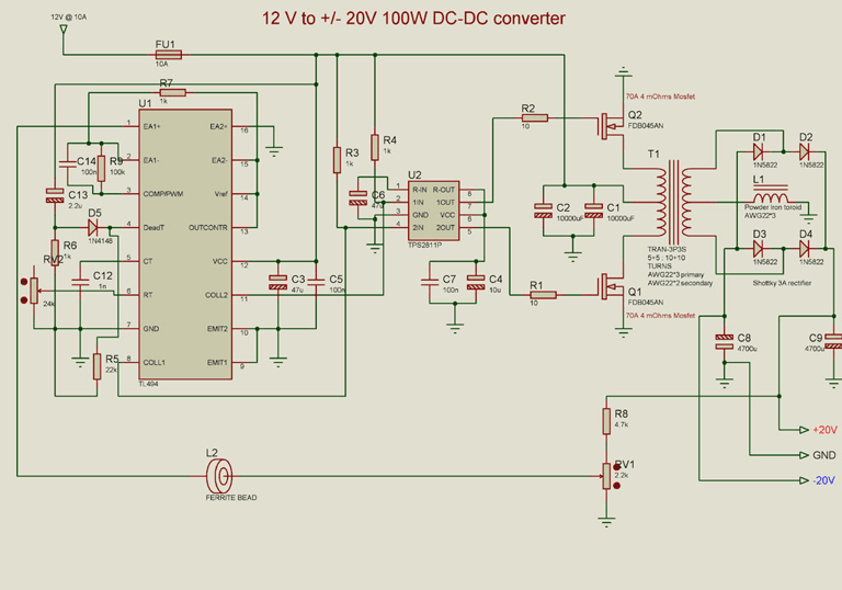
A DC to DC converter circuit is designed to convert a DC voltage to another DC voltage with different levels. This specific converter transforms a +12 V DC input into a symmetrical output of +/-20 V DC. Such circuits...
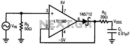
This closed-loop peak detector circuit utilizes a Schottky diode within the feedback loop to achieve high accuracy. The 20-ohm resistance RQ serves to isolate the 0.01-ohm load and prevent oscillations. The direct current (DC) value is measured using a...
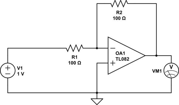
Considering a simple circuit as illustrated below, when the voltage source activates suddenly (changing from 0V to 1V), current will flow through the resistor R1. Assuming an ideal operational amplifier (op-amp) that draws no current, and an ideal voltmeter...
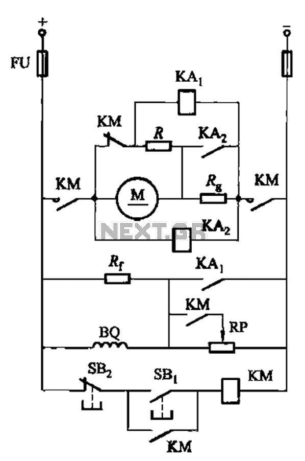
The circuit illustrated in Figure 3-197 features a dish adjust rheostat (RP) that allows for the adjustment of field current, which in turn modifies the motor speed. The circuit operates by utilizing a rheostat, which is a variable resistor that...
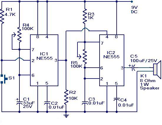
The primary component of this circuit is a doorbell utilizing two NE555 timer ICs. When the switch S1 is momentarily pressed, the speaker produces a bell sound, which is determined by the time period of the monostable multivibrator configured...
Two circuits for laser transmitters are described. The first circuit utilizes a simple laser pointer module, with 3 or 5mW devices functioning effectively. Higher power units are often imported from the USA or Hong Kong compared to UK approved...