
JFET PREamp

The circuit described is a low-noise preamplifier utilizing an N-channel JFET as the input stage, followed by a PNP transistor for signal amplification and an NPN transistor configured as an emitter follower for output. The JFET's selection is crucial, as it determines the output bias voltage, which is essential for optimal performance. The input resistor R1 plays a significant role in ensuring the JFET operates in its desired region by reverse-biasing its gate, while R2 establishes the quiescent current for the PNP transistor, allowing for stable amplification.
The feedback mechanism in the circuit ensures that the current through the input transistor remains nearly constant, which is vital for maintaining performance across varying signal levels. The omission of the PNP load resistor enhances the circuit's gain and reduces noise, demonstrating the importance of component selection and configuration in circuit design.
The output stage, utilizing an emitter-follower configuration, provides a buffered output while limiting the maximum output voltage swing. The output pull-down resistor R3 is essential for defining the load characteristics and impacts power consumption, highlighting the trade-off between performance and efficiency in battery-operated applications. The design effectively balances these factors to achieve a reliable and efficient low-noise audio preamplifier suitable for various applications.The input transistor Q2 is an N-channel JFET. Each particular JFET sets a particular output bias voltage, so the JFET must be selected from among multiple devices for the desired bias value. Fortunately, due to the low current involved, desirable devices can come from a wide range of device types.
JFETs also vary with respect to gain and noise lev el, so best operation requires some selection there as well. However, other than exceptionally bad noise in particular devices, a wide range of JFETs function surprisingly similarly. The input resistor R1 just drags the JFET gate to ground potential and so reverse-biases the FET. The value should be at least 10x the signal source impedance, but probably could be as high as 100 megohms, if that was useful for some reason.
Larger resistors do produce somewhat more Johnson noise, but that is normally "shunted" or "shorted out" by a low-impedance signal source. The second transistor Q3 is a bipolar PNP. One might think to make it a low-noise low-current-linear device, but in practice that does not seem to matter much.
Many different PNP devices can be used with no circuit change and remarkably little difference. The resistor across the base-emitter junction of the PNP R2 sets the "standing" or "quiescent" current for the input transistor. The PNP operates on the "knee" of turn-on, at about 0. 6V. The recommended value of 5K allows about 0. 6/5k = 120uA to flow through the JFET before the PNP starts to turn on, which then increases the output voltage and starts to turn off the input transistor.
Since feedback keeps the current through the input transistor almost constant, resistor R2 can be seen as a particularly simple form of constant-current source. The low operating current allows the JFET gate to operate at a bias voltage much lower than the specified "Gate-Source Cutoff Voltage, " thus making a wide range of devices usable.
The best JFET current for lowest noise can easily be checked by varying the PNP base-emitter resistor value. The current in the second transistor typically is much lower than in the input transistor. That typically reduces the gain we can expect from the second transistor. The PNP load resistor is missing. The original design, and every other design I have seen, had a load resistor to ground. However, removing that resistor seemed to produce more gain and less noise. The current in the second transistor apparently works against a larger load resistance to produce a larger voltage result.
The results seem fairly independent of device characteristics, and the circuit without the resistor simulates just fine. The output transistor Q1 is a bipolar NPN as an emitter-follower, and is also noncritical. For example, a high-gain Darlington device increased the open-loop gain by all of 3dB, and had even less effect on the closed-loop gain.
The emitter-follower output does reduce the maximum positive output by 0. 6V. So if we expect to work well with a 4V supply (a 9V battery at end-of-life), we have a maximum output of 3. 4V. That means, ideally, we would want the output bias to be around 1. 7V, although we can vary that with minimal impact. The output pull-down resistor R3 provides the energy for negative-going parts of the audio output. Since the emitter-follower can only source current, this resistor will define the maximum load which can be driven in a negative direction.
Thus, it should be small, typically under 1/10 the input resistance of the next stage. However, this resistor also is one of the main contributors to power consumption, so it also should be large. If the output bias is set (by selecting the FET) at 1. 5V, a value of 1K will sink about 1. 5mA which the battery must then supply whenever the preamp is operating. Battery life for a new 9V alkaline battery with a 2mA load should be about 330 hours (13. 75 days or about 2 weeks) of continuous operation. Less current means better battery life. Po 🔗 External reference
Related Circuits

The circuit functions adequately, although it is not ideal in terms of quality. However, there is a minor issue when interfacing the output with an Arduino. The output swings below ground, meaning it is biased at 0V, while the...
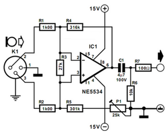
The preamplifier is designed for use with dynamic (moving coil MC) microphones with an impedance of up to 200 ohms and balanced terminals. It features a straightforward design and can be regarded as a single-stage instrument amplifier utilizing a...
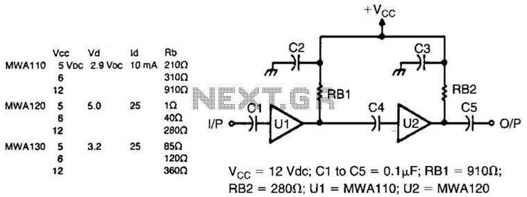
Motorola MWA 110, 120, or 130 are wideband amplifier ICs. This wideband preamp circuit can be used in many applications. Keep the leads short when constructing the circuitry. PC board layout (shading represents copper) and parts layout. X is...
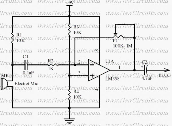
This circuit will be useful if you have an electret microphone that produces a low audio (sound) level and you want to connect it to an amplifier or something like it. The circuit boosts the microphone output voltage to...
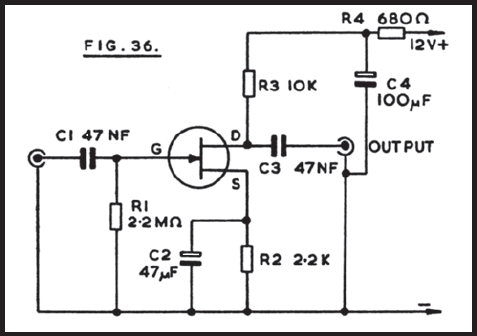
Figure 36 illustrates the circuit of a preamplifier featuring a high impedance input and an output circuit designed for coupling to a main amplifier. This configuration is particularly advantageous for applications such as amplifying the signal from a crystal...
The three circuits were based on the vacuum tube ECC83, designed to produce phono preamplifiers in compliance with RIAA standards. The described circuits utilize the ECC83 vacuum tube, a dual-triode component known for its low noise and high gain characteristics,...