
L4960 by a monolithic switching power supply

The L4960 is a highly integrated switching regulator that is designed to provide a stable output voltage from a varying input voltage. The operation begins with the AC mains voltage being stepped down by a transformer to a lower AC voltage, which is then rectified by a bridge rectifier into DC voltage. This DC voltage is filtered to smooth out any ripples, providing a steady input voltage (Vi) for the L4960.
The internal soft-start feature of the L4960 is crucial for preventing inrush current that can damage components during the initial power-up phase. By gradually increasing the output voltage, the circuit ensures that the connected load is not subjected to sudden surges of current. The feedback mechanism involving resistors R3 and R4 plays a vital role in maintaining output voltage regulation. The sampled voltage is compared to a precise reference voltage of 5.1V, and any deviation results in an error voltage that drives the PWM comparator.
The PWM comparator modulates the width of the output pulses sent to the power output stage, which consists of a switching power MOSFET. This modulation effectively controls the amount of energy transferred to the output load. The energy storage components, including the inductor L and capacitors C6 and C7, work together to smooth out the output voltage, ensuring that it remains constant despite variations in load current.
The current spreading circuit enhances the L4960's output capability, allowing it to handle higher current loads up to 10A. This is achieved through the addition of an external power transistor that shares the load current, preventing overheating and ensuring reliable operation. The over-current protection circuit is a critical safety feature that prevents damage to the L4960 and connected components. When the output current exceeds the threshold of 10A, the circuit activates, clamping the voltage at the L4960's pin to 0V, effectively disabling the PWM control and stopping the output current flow to protect the system from damage.
In summary, the L4960 switching power supply circuit is designed for efficiency and reliability, with built-in features for voltage regulation, current sharing, and over-current protection, making it suitable for a variety of applications requiring stable power delivery. As shown in FIG constituted by L4960 + 5 ~ + 40V switching power supply circuit. AC 220V voltage through the step-down transformer, bridge rectifier and filter DC voltage Vi, i nput L4960 O feet, under the action of L4960 internal soft-start circuit, the output voltage gradually increased. When the entire internal circuit is functioning normally, the output voltage in R3, R4 after sampling returned feet, internal error amplifier is compared with a 5.1V reference voltage to obtain the error voltage, then the magnitude of the error voltage to control the PWM comparator the pulse width, the power output stage after amplification and step-down output circuits (constituted by L, VD, C6 and C7), the output voltage Vo remains constant.
L4960 7 feet get is power pulse modulation signal, which is high (L4960 internal switching power MOSFET) when, in addition to the load, as well as part of the energy stored in L and C6, C7, in which case freewheeling VD deadline. When power low-power pulse signal (switching power MOSFET is off) when, VD conduction, stored in L on through the loop formed by VD configured to load discharge, thereby maintaining the output voltage Vo constant.
Figure (c) shows a current spreading circuit L4960. This circuit uses an external power transistor approach. The output current is extended to 10A. And over-current protection circuit is provided by the VT2, VT3 and R5, R6, R7, R8, R9 other components, when the output current is greater than 10A, the protection circuit, the potential of the L4960 foot clamp to 0V, closed PWM comparator terminates the output current.
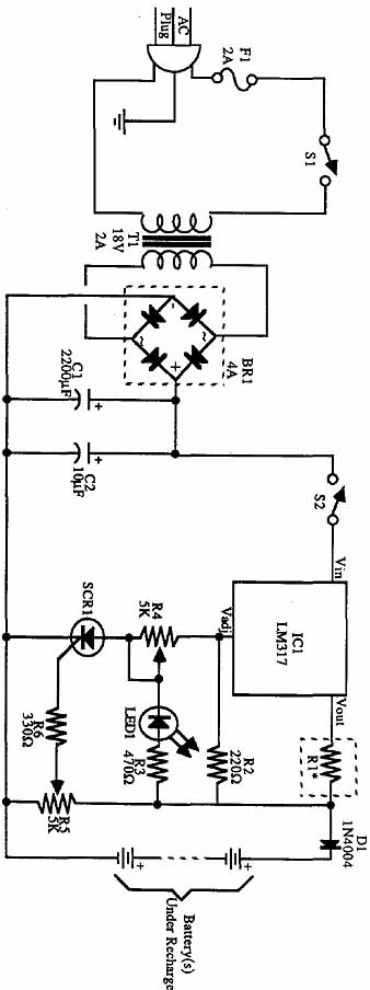
Related Circuits
The incoming AC is routed to the primary terminals of a 12.6-volt transformer. The hot side of the AC is connected through a fuse and a single-pole single-throw (SPST) toggle switch. When the switch is in the OFF position,...
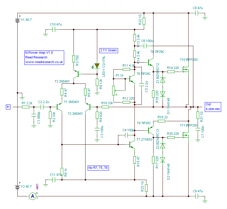
The amplifier has been designed as an ideal upgrade for builders looking to advance from Gainclones. This amplifier delivers power where Gainclones may struggle, while still producing a pleasant sound. The implementation of n-channel MOSFETs in the output stage...

A siren circuit diagram that generates a strong, high-power siren or alarm sound using complementary transistor pairs BC 557 and BC 337, arranged as an oscillator. The described siren circuit employs a pair of complementary transistors, BC 557 (a PNP...

The circuit depicted in the figure is designed to achieve a higher power output by modifying specific components. On the left side of the figure, components R1, L1, D1, and capacitors C1 to C7 form a conventional filtering and...

This simple circuit provides a regulated output of 4.7 volts for charging mobile phones. A USB outlet delivers 5 volts DC at a current of 100 mA, which is adequate for slow charging of mobile devices. Most mobile phone...

The ADSP-2103 and ADSP-2105 are digital signal processors that interface with the AD7714. When the output is active, the ADSP-2103/2105 configuration includes the RFS non-TES non-terminal set to a low level, while the SCLK terminal is configured for serial...