
linearizing circuit for thermocouples
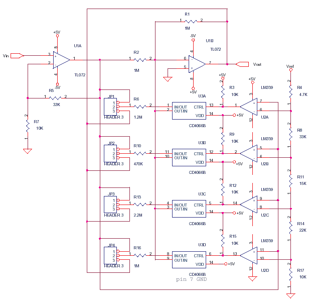
The circuit operates by utilizing two operational amplifiers, U1A and U1B, where U1A functions as a buffer to ensure that the input signal is adequately amplified before it is processed by U1B. The gain of U1B is adjusted through the manipulation of resistors that are switched in and out of the circuit by the 4066 multiplexer. This multiplexer allows for precise control over the gain settings, enabling the circuit to achieve different gain levels as required for various applications.
The LM339 comparator plays a critical role in this circuit by providing reference points for the switching of the gain resistors. It compares the buffered input signal against predetermined reference voltages. Based on this comparison, the LM339 controls the state of the 4066 multiplexer, effectively changing the configuration of the gain resistors connected to U1B. This switching mechanism is essential for achieving the desired amplification or attenuation.
The use of jumpers JP1 to JP4 allows for user-defined selection of gain settings, making the circuit versatile for different transducer types and applications. The configuration of the resistors switched by the 4066 can be adjusted to either amplify the signal through R1 or attenuate it through R2, depending on the specific needs of the application. Overall, this circuit design is suitable for applications requiring precise signal conditioning from transducers, providing flexibility and adaptability in gain settings.This circuit changes the gain of opamp U1B in four steps or segments. It can be used to get a linear output from most transducers to 1% levels. U1A is a amplifying buffer use it to boost the signal to the required level. The resistor values i have put are for an imaginary transducer, you have to design them. The buffered input signal is compared to reference switching points by LM339. LM339 changes the gain resistors of U1B thru the mux switch 4066. JP1 to JP4 can select either amplification or attenuation of signal. The resistor switched by 4066 can be across R1 or R2 based on JP1 to JP4. 🔗 External reference
Related Circuits
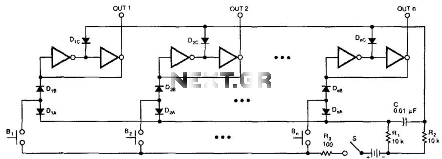
This switching circuit functions as a bank of interlocked mechanical switches. Activating one of the buttons latches its corresponding output while unlatching a previously selected output. A pair of inverters creates a latch for each output. For instance, pressing...
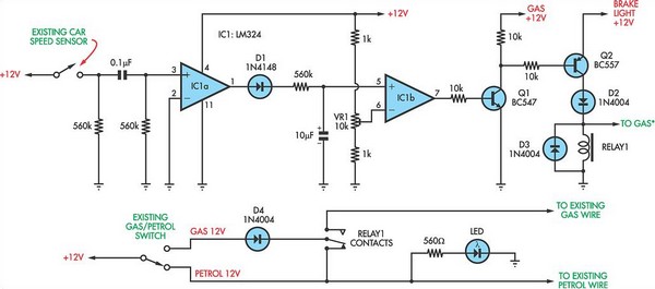
The following circuit illustrates a petrol gas switch sensor circuit diagram designed for a Pajero vehicle. It features a simple configuration utilizing the LM334 integrated circuit and operates automatically. The petrol gas switch sensor circuit is designed to monitor and...
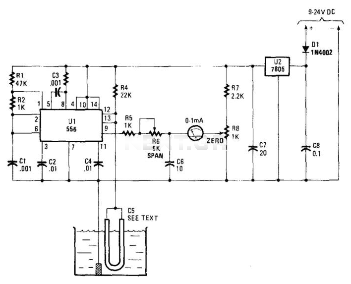
Using a capacitor sensor to detect water levels is a straightforward sensing method. This circuit employs C5, which consists of 10 to 20 inches of #22 enameled wire as one of the electrodes. The oscillator, an NE556 timer, experiences...
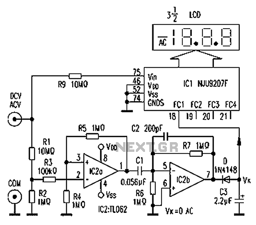
The circuit depicted in the figure illustrates an automatic AC/DC converter for a digital multimeter. Typically, standard digital multimeters require manual intervention to switch between AC and DC measurements. The new DT860D digital multimeter utilizes the NJU9207F automatic range...
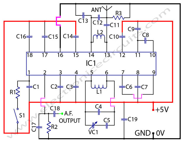
The TDA7000 is a monolithic integrated circuit designed for mono FM portable radios or receivers, emphasizing minimal peripheral components for compact size and cost-effectiveness. This integrated circuit features a Frequency-Locked-Loop (FLL) system with an intermediate frequency of 70 kHz....
The motor winding is configured with delta transposition capacitance, designated as cl-C-3G. It operates as a DC LAN speed generator and is associated with a three-phase asynchronous motor, which is coaxially connected through a field winding powered by a...