
Switching Circuit

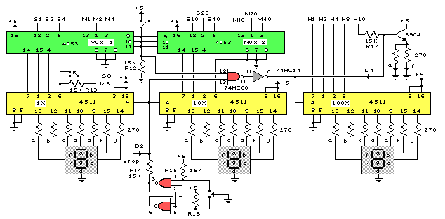
This switching circuit operates on the principle of interlocking outputs, ensuring that only one output remains active at a time, akin to a mechanical switchboard. The circuit includes a series of latches formed by pairs of inverters, which are crucial for maintaining the state of each output. Each button press generates a positive pulse that triggers the corresponding latch.
The operation begins when button Bl is pressed. This action sends a positive pulse through resistor diode D1B to the latch associated with OUT1. The inverter pair linked to OUT1 then sets this output high, and due to the feedback loop created by the inverters, OUT1 remains in this HIGH state until another button is pressed.
The circuit's design includes a differentiating stage composed of capacitor C and resistor R2. This stage serves to shorten the duration of the pulse generated by the button press. The shortened pulse is distributed to all the latches within the circuit. However, only the latch that receives the longer setting pulse remains unaffected by the resetting action, allowing it to stay latched while others are reset. This mechanism effectively prevents multiple outputs from being active simultaneously, maintaining the integrity of the switching function.
In scenarios where multiple buttons are pressed at the same time, the circuit's design allows for the potential of multiple outputs being latched. This feature can be advantageous in applications requiring simultaneous activation of multiple outputs, although it may deviate from the intended single-output functionality. Overall, the circuit is designed to provide a reliable and efficient method of controlling outputs through a simple button interface, ensuring that the operation remains intuitive and straightforward. This switching circuit acts like a bank of interlocked mechanical switches; pushing one of the buttons latches its corres ponding output and unlatches a previously selected output. A pair of inverters forms a latch for each output. Pressing button Bl, for example, applies a positive pulse, via resistor diode DIB, to the input of the first output"s, OUT1, latch. This positive pulse will set OUT1 high. Feedback locks OUTl"s pair of converters in this HIGH state. Meanwhile, the pulse will also pass through diode D1A to the differentiator that is formed by C and R2.
The differentiator will shorten the pulse. The shortened pulse goes to all the latches and resets all of them, except the latch that sees the longer setting pulse. Obviously, if you press more than one button at once, more than one output will latch at once.
Related Circuits
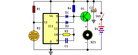
This circuit is housed in a compact enclosure and is positioned within the refrigerator, either near the lamp or at the door opening. When the refrigerator door is closed, the interior remains dark, causing the photoresistor R2 to exhibit...
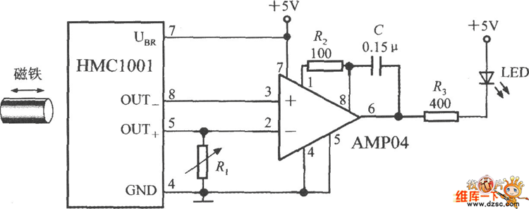
The image depicts a proximity switch circuit that includes the HMC1001 Hall effect sensor, an operational amplifier (AMP04), and a light-emitting diode (LED). In this configuration, the operational amplifier functions as a comparator. When a magnet with a length...
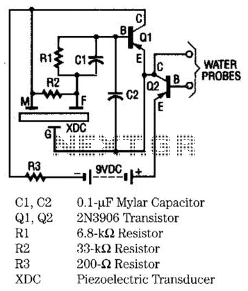
The moisture detector utilizes two transistors and a piezoelectric transducer to emit an alarm tone when water is detected. Transistor Q1 functions as a crystal-controlled oscillator, employing a portion of the piezoelectric transducer XDC, which consists of two piezoelectric...
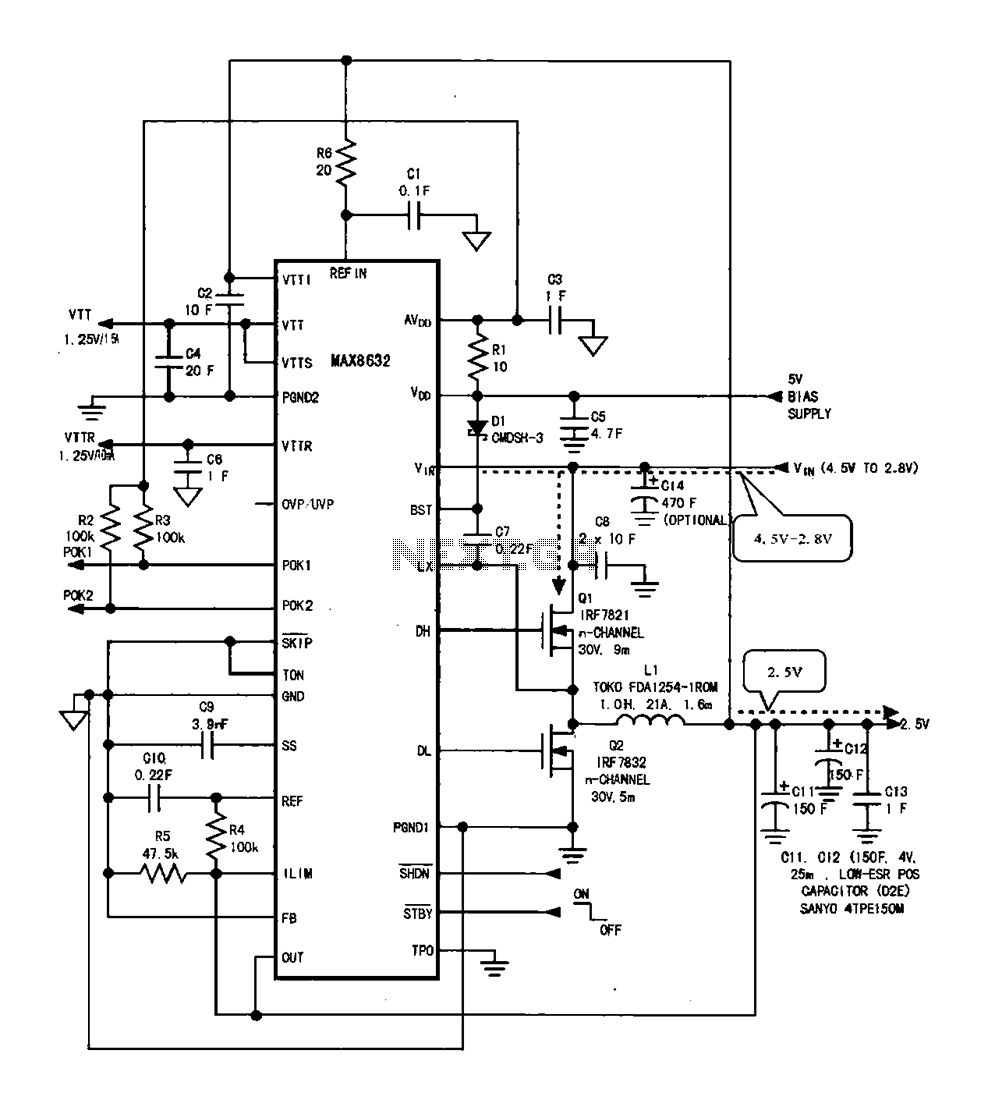
DDR memory power supply circuit. This circuit illustrates the power supply configuration for notebook DDR memory, utilizing the MAX8632 power control circuit chip. The power supply terminal VDD is connected to the voltage detection point 1. The battery DC...

When the circuit is initially powered, neither transistor is activated, resulting in high base voltages for both and a tendency to turn on. Due to slight asymmetries, one transistor will activate first, leading the circuit into one of its...
This device is a combination digital clock timer and solar panel charge controller designed to maintain a deep cycle battery charged by a solar panel. The timer output controls a 12-volt load for a 32-minute interval each day. The...