
LM1894 Principles and Applications a

The LM1894 is a sophisticated integrated circuit designed for dynamic noise reduction applications. It employs a dual-path architecture for processing audio signals, allowing for simultaneous handling of left and right channels. The core of the device consists of a variable gain amplifier (A2) that adjusts the gain of the incoming signals based on the detected noise levels. This amplifier is crucial for maintaining audio fidelity while minimizing unwanted noise.
The mixed signals from the left and right inputs are fed into an adder circuit (A3), which combines them for further processing. The subsequent amplification stage (As) enhances the signal strength, ensuring that the noise reduction mechanism operates effectively. The peak detector plays a vital role in extracting the control voltage that informs the system about the signal's amplitude.
This control voltage is essential for the dynamic adjustment of the main channel bandwidth. The built-in voltage/current converter translates the control voltage into a corresponding control current, which modulates the bandwidth according to the characteristics of the input signals. The design allows for greater bandwidth when the input signal contains a rich frequency spectrum, facilitating the preservation of audio quality during noise reduction.
The operational parameters of the LM1894 are finely tuned to respond to varying signal conditions. Specifically, the relationship between control current and bandwidth is designed such that a decrease in control current results in a significant increase in bandwidth, enhancing the circuit's ability to process a wide range of audio frequencies. This adaptability makes the LM1894 an effective choice for applications requiring high-quality sound reproduction while minimizing noise interference.A typical representative of the dynamic noise reduction by the United States National Semiconductor first be successfully developed and integrated LM1894 (see Table 1-3), the u pper part of the figure 1-1070 its principle is shown in the left and right the same two a main signal path, the left and right input signals respectively, by 132 feet and after the noise reduction processing is output from 11,4 foot. Between the input and output, A2 constituted by the variable gain OdB and band-pass cut-channel control of the low-pass filter o the lower part of the figure as Vice signal control channel, a shared control channel around here, it will help simplify the circuit.
First in the left and right input signals are mixed into the adder A3 all the way, and then the deputy - amplification and signal amplifier As, VD group after a peak detector detector 10 feet to get a DC control voltage, and then by the built-in voltage/current (V /,) converter into a DC control current to Ai to change the main channel bandwidth. Press the noise reduction design requirements, the input signal frequency component richer, the greater the DC control voltage is converted into a DC control current is smaller, the corresponding main channel bandwidth wider.
Specifically, the control current is decreased by 1 per belly to increase bandwidth 27Hz. Conversely, when the input signal into a high frequency, the less points, the narrower the bandwidth of the main channel, typically 800Hz ~ 1,1 seven o
Related Circuits

This article offers valuable information for creating a specific oscillator or pulse generator using integrated circuits (ICs), resistors, and capacitors, regardless of the version of the 555 IC utilized. The 555 timer IC is a versatile component widely used in...
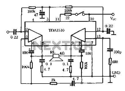
TDA1510 is an audio power amplifier from Philips. This integrated circuit (IC) includes features such as load short protection, open load detection, and an overheat protection circuit. It offers stable output voltage, excellent ripple rejection performance, requires fewer external...
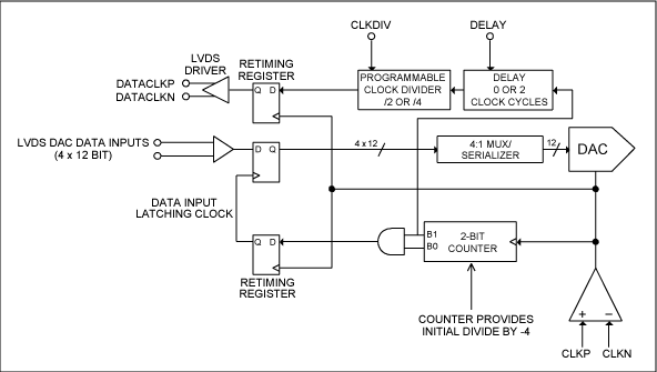
This application note provides insight into how to synchronize multiple high-speed DACs in transmitter applications. This document outlines the techniques and methodologies for synchronizing multiple high-speed Digital-to-Analog Converters (DACs) in various transmitter applications. Synchronization is crucial in systems where multiple...
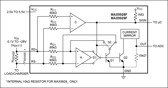
This article compares high-side and low-side amplifiers used for measuring battery charging currents. It recommends selection criteria for current-sense resistors and describes a high-voltage circuit breaker designed for overcurrent protection. High-side and low-side amplifiers are essential components in battery management...

The ability of an SCR to control large currents to a load using a small gate current makes the device highly useful in switching and control applications. Several potential applications for the SCR include power control, switching, zero-voltage switching,...

Power demand in portable designs can require, in specific applications, more than 1 A. A method involves paralleling two DC to DC converters on the same load instead of using a single higher current converter with a lower switching...