
Logic Probe With Sound

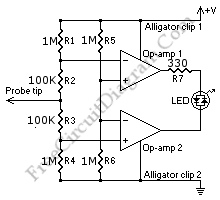
The logic probe circuit is designed to provide visual and audible feedback for digital signals, making it a versatile tool for troubleshooting and testing electronic circuits. The selection between TTL and CMOS logic levels allows for flexibility in applications, as different digital devices may operate on different voltage levels.
The use of a window comparator, implemented with operational amplifiers IC1a and IC1b, ensures that the logic probe can accurately differentiate between high and low logic levels. The resistors connected to switch S1 are critical in defining the threshold voltages that determine the logic state, thus allowing for precise operation in various environments.
When the probe is in an open-circuit condition, the midrange value established by the 1.2M and 680k resistors keeps both LEDs off, indicating that no signal is present. This feature is important to avoid false readings when the probe is not in contact with a circuit.
Upon detecting a pulse signal, IC1a's output toggles the clock input of flip-flop IC2a, which in turn controls LED3. The option to configure LED3 to either blink with each pulse or remain lit continuously provides users with a choice based on their monitoring needs. This adaptability enhances the usability of the probe in different testing scenarios.
Furthermore, the integration of diodes D5 and D6 in the circuit protects the integrity of the signals being fed to transistor Q1, which is responsible for resetting flip-flop IC2b. The piezo sounder connected to the outputs of IC2b provides an audible indication of the pulse signal, which can be particularly useful in noisy environments where visual indicators may be overlooked.
Overall, this logic probe circuit is an effective solution for monitoring digital signals, combining visual and audible indicators for enhanced functionality in electronic diagnostics.This logic probe can be selected to operate on TTL or CMOS logic levels, depending on switch S1. A string of resistors associated with switch S1 sets the threshold levels for a window comparator comprising IC1a and IC1b. Depending on whether the level applied to the probe is high or low, the window comparator turns on LED1 (high) or LED2 (low).
Th e 1. 2M and 680k resistors set the probe signal to a midrange value when the probe is open-circuit, thereby preventing either LED from being lit. If a pulse signal is present, the output of IC1a will toggle the clock input of flipflop IC2a. This drives LED3 which either lights for each pulse or continuously, depending on the setting of switch S2.
Finally, the outputs of IC1a & IC1b are connected by diodes D5 & D6 to the base of transistor Q1 which is connected to the Reset input of flipflop IC2b. This has a piezo sounder (not buzzer) connected between its Q and Q-bar outputs so that it produces a sound which echoes the input pulse signal.
🔗 External reference
Related Circuits
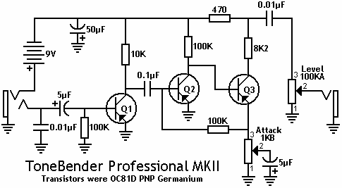
This is probably one of the most legendary fuzz pedals that has ever existed, and for good reason too! This thing can produce some completely saturated fuzz that is capable of slipping into feedback easily if you crank it...
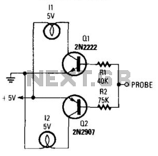
By connecting this circuit to a powered logic device, an indication of its status can be obtained. If the circuit is open, neither of the test lamps will illuminate. If the circuit is grounded, the low (or zero) lamp...
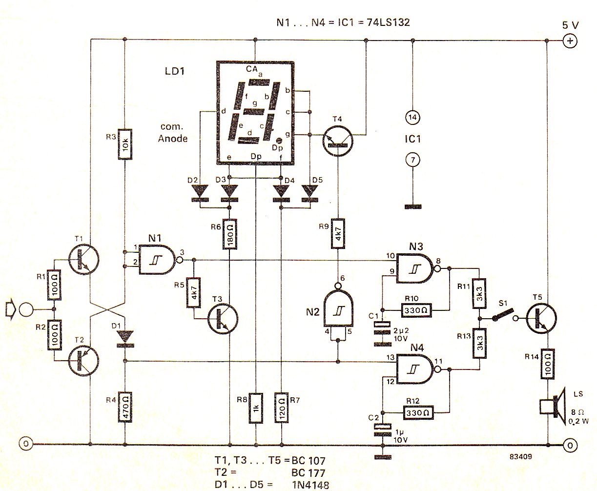
When the input signal is at logic high (1), the display indicates `H`, and the loudspeaker emits a note that is one octave higher than the low tone. The operation of the circuit can be observed in the circuit...
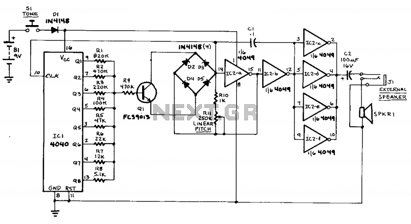
This circuit can generate sounds such as a European police-car siren, bird noises, and spaceship sounds. It can also function as a doorbell or an alarm. The circuit consists of four main components: a binary counter, a digital-to-analog (D/A)...
This is a simple circuit of a Logic Probe for tri-state logic. This circuit can be built in just a few hours. Additionally, this circuit has other features. The Logic Probe circuit for tri-state logic is designed to detect and...
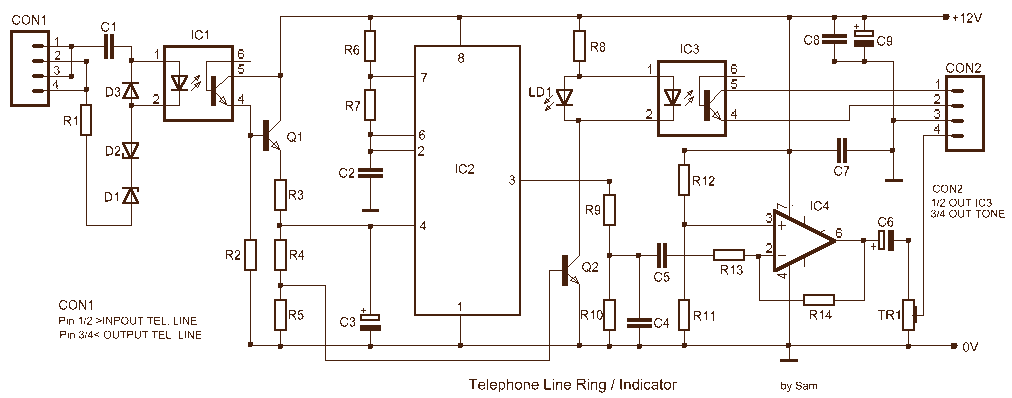
It is a relatively simple circuit, with which we can have optical and sound clue, when we have telephone ring in the line of telephone. The calls in the line, are changed in pulses of frequency 400 HZ from...