
Low-Frequency Crystal Controlled Oscillator

The described circuit functions as a precise low-frequency sine wave oscillator, ideal for testing low-frequency quartz crystal units. The design’s reliance on low-cost components, such as AF bipolar transistors and a JFET, makes it accessible for various applications. The automatic adjustment of the loop gain through Q3 ensures consistent performance across the specified frequency range while minimizing distortion. The isolation provided by Q4 and Q5 is crucial for maintaining signal integrity, preventing non-linear effects from impacting the output. The feedback mechanism established through the JFET enhances the circuit’s robustness against power supply variations, which is particularly beneficial in laboratory settings where environmental conditions may fluctuate. The ability to adapt the circuit parameters, such as the resistor values based on frequency, allows for fine-tuning according to specific operational requirements, making this design a reliable choice for RF engineers seeking to evaluate quartz crystal units effectively.The RF engineer sometimes has to look for an instrument that will check a low frequency quartz crystal unit reliably and rapidly. This is a difficult piece of equipment to find and the engineer often has to consult an electronic circuits handbook for the schematic of a circuit that will perform the task.
Unfortunately, there aren`t many such circu its in the technical literature currently available, and when found, they don`t always work as expected. A circuit that has been found to work at full satisfaction in the frequency range from 10 kHz to 500 kHz is illustrated in Figure 1.
This is a schematic of a low frequency sine wave oscillator featuring low distortion, wideband operation and crystal control. The circuit, originally developed for laboratory use, employs low cost AF bipolar transistors for the oscillator and amplifier sections and a JFET for loop-gain control.
Operation of the oscillator in the 10 kHz to 500 kHz frequency range has been found to be excellent, while measured distortion is kept under 0. 1 percent. Q1, Q2 and associated circuitry form a modified astable multivibrator in which the loop gain is automatically adjusted to the threshold of oscillation by means of field effect transistor Q3.
Q4 linearly amplifies the signal present at the collector of Q2 and isolates the oscillator section of the circuit from the output. This stage features wideband operation and delivers a clean 2. 5 Volt amplitude sine wave into a resistive load greater than or equal to 20 kohms. The stage comprising Q5 has a voltage gain of 1 and its sole purpose is to isolate the non-linear effects of rectifier D1 from the output.
Transistor Q4 also amplifies the minor changes in amplitude of the oscillator`s waveform due to temperature effects and/or power supply variations, so a magnified version of the perturbance is fedback to rectifier D1 producing a corresponding change in Q3`s gate voltage. This action modifies the FET`s drain-source resistance and hence adjusts the loop gain to a new value slightly above unity, just enough to maintain a constant amplitude in the output.
Figure 2 shows optimum values for capacitor C according to the crystal`s resonant frequency. Extra gain is needed from transistors Q1 and Q2 at frequencies below 40 kHz. This is due to the fact that low frequency crystals exhibit large values of series resistance, affecting loop gain (Table 1 compares typical values of series resistance for low frequency units). According to what has been stated, resistor R is made 10 kohms for frequencies under 40 kHz. Above this value, 1 kohm will do. 3) Due to the dynamic action of the JFET the output level is almost insensitive to power supply variations.
The 3. 3 Volt zener diode further enhances this result. 🔗 External reference
Related Circuits
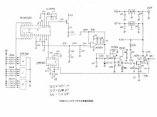
This MOT's LSI is highly suitable for designing VFOs in ham radios, featuring a 4-digit BCD preset counter with a range from 3 to 3999. It also includes a standard crystal frequency oscillator and preset dividers. The input nodes...

The Colpitts Oscillator is characterized by tapping the mid-point of the capacitive side of the oscillator section. The inductor can be the primary side of a speaker transformer. The feedback comes via the inductor. The Colpitts Oscillator is a type...
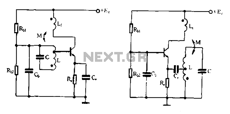
Base frequency selection, frequency-selective emitter type transformer coupled oscillator circuit The described circuit is a transformer-coupled oscillator that utilizes an emitter type configuration to achieve frequency selection. This type of oscillator is designed to generate signals at specific base frequencies,...
A Pierce Oscillator is a type of oscillator that utilizes a crystal instead of a parallel-resonant circuit (LC circuit). This oscillator also employs the voltage developed from a tap between two capacitors in the tank circuit. Both Pierce Oscillators...

A DTL integrated circuit comprises a crystal oscillator, which is represented by the integrated circuits. The oscillation frequency ranges from 100 kHz to 1 MHz. Additionally, it includes a gate circuit that supplies a signal for the DTL oscillator...
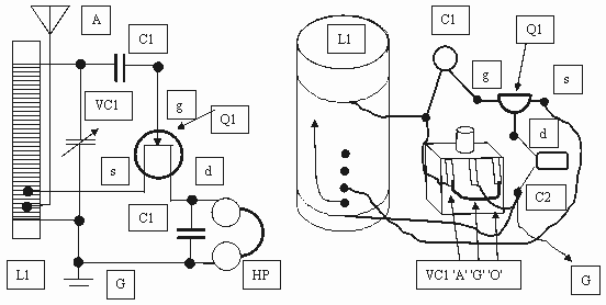
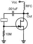
The source connection is tapped into the tuning coil low down, as a means of impedance matching with the headphones and acts as the anode, while the drain connects with your headphones as the cathode, to complete the detector...