
Low-Level Power Fet Driver Method

This circuit is designed to operate within a voltage range of 16 to 50 volts, making it versatile for various applications. The inclusion of a buffer circuit, indicated within the dashed lines in the schematic, enhances the performance by achieving switching times as low as 100 nanoseconds. In its standard configuration, the circuit achieves a switching time of approximately 1 microsecond, which is adequate for many applications but can be improved.
The core of the circuit consists of a transistor (Q1) and a resistor (R1), which together function as a switched current source. This current source is capable of delivering around 12 milliamperes (mA) to the load. The current then passes through another resistor (R2), which regulates the voltage supplied to the field-effect transistor (FET) at 12 volts. This configuration allows the circuit to maintain stable operation across a broad spectrum of supply voltages, ensuring reliable performance even in the presence of significant voltage ripple and noise.
To optimize the switching time, it is possible to reduce the values of resistors R1 and R2. However, this modification comes with a trade-off, as it results in increased power dissipation within both the resistors and the transistor Q1. Therefore, careful consideration must be given to the thermal management of these components when adjusting their values.
Alternatively, the implementation of a buffer circuit can significantly enhance the switching speed to 100 nanoseconds while maintaining low power dissipation levels. This is particularly advantageous in applications where rapid switching is critical, and power efficiency is a concern. Overall, this circuit design provides a robust solution for applications requiring reliable switching performance across varying supply conditions. This circuit operates from a 16- to 50-V supply. Adding the buffer circuit (within the dashed lines) offe rs 100-ns switching times. Otherwise, the circuit switches in 1 /xs. Ql and R1 form a switched current source of about 12 mA. The current flows through R2, which supplies 12 V to the FET. The circuit works well over a wide range of supply voltages. Furthermore, it switches smoothly in the presence of large ripple and noise on the supply. The switching time (about 1 /as) can be reduced considerably by lowering the values of Ri and R2 at the expense of higher power dissipations in the resistors and Ql. Alternatively, a buffer circuit can be added to produce switching times of 100 ns without generating significant power dissipation.
Related Circuits

A battery switch-over circuit is being developed, consisting of two parallel lanes as depicted in the circuit diagram. The operational voltage range spans from 3V to 12V. Only one lane should be active at any given time, which is...
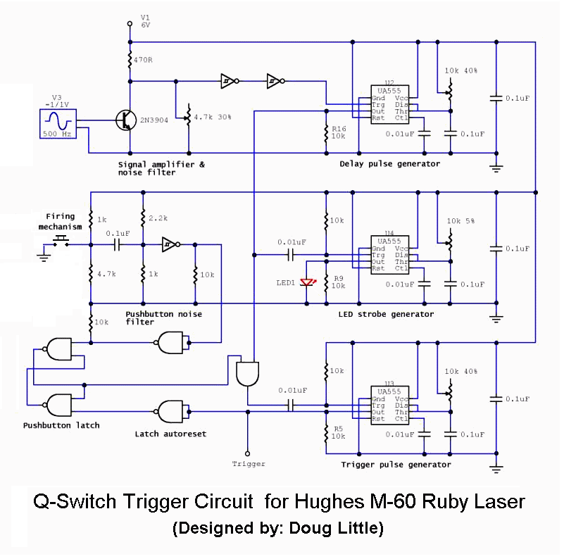
This chapter contains circuit diagrams for several power supplies designed for pulsed solid-state lasers. These include units suitable for driving the widely used Hughes ruby and YAG rangefinder laser assemblies, one utilizing the flash from a disposable pocket camera,...

The design of the AC to DC front stage boost converter in discontinuous mode involved several steps. Initially, the specifications were defined. Subsequently, research was conducted, and the basic power factor correction circuit was analyzed. Finally, the boost converter...
The current design of a power inverter offers an efficiency of approximately 85% and a power output exceeding 200 watts. This document provides a complete circuit schematic and detailed building procedure for a home-built power inverter. While numerous articles...
Arduino can drive various types of motors. However, the low-power signals from Arduino must control high-power circuits to operate the motors effectively. This document will provide examples of how Arduino can control different motor types and sizes. A motor...

Whenever there is a need for battery-powered lighting, such as for camping, solar-powered cottages, cars, boats, planes, or emergency situations, fluorescent lamps are highly appealing. They are significantly more efficient than incandescent lamps, producing much more light for less...