
making 25w low power inverter circuit

The 555 timer is a versatile integrated circuit widely used in timer, pulse generation, and oscillator applications. In the astable mode, the timer continuously switches between high and low states, generating a square wave output. The frequency of oscillation is determined by the values of resistors R2 and capacitor C1, which set the charge and discharge times of the timing capacitor.
The output from the astable oscillator is taken from pin 5, which provides a square wave signal. This output can drive other components or circuits directly, depending on the load requirements. The second section of the 555 timer acts as a phase inverter, which is crucial for applications requiring signal inversion or phase shifting. The output from this section is available at pin 9, allowing for further signal manipulation or interfacing with other circuit elements.
Resistors R3 and R4 play an essential role in maintaining the stability of the circuit. They are connected to the outputs of transistors Q1 and Q2, ensuring that these outputs do not excessively load the oscillator. This configuration helps maintain the integrity of the oscillation frequency while preventing distortion that could arise from improper loading conditions.
In summary, this configuration of the 555 timer as an astable oscillator with a phase inverter provides a reliable means of generating and manipulating pulse signals. The careful selection of component values and the inclusion of load-resisting elements ensure robust performance across various electronic applications.The first section of the 555 timer is wires as an astable oscillator with R2 and C1 setting the frequency. The output is available at pin 5. The second section is wired as a phase inverter. That output is available at pin 9. Resistor R3 and R4 keep output transistor Q1 and Q2 from loading down the oscillator. 🔗 External reference
Related Circuits

The circuit utilizes a transistor (VT) and a voltage regulator (VSL) to create a constant current source, employing three regulators to enhance the performance of the regulator circuit. The described circuit employs a transistor (VT) in conjunction with a voltage...
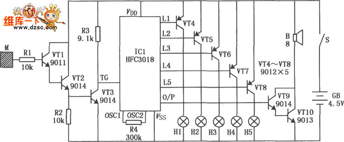
The circuit diagram for a dynamic toy that produces eight sounds and five flashing lights is illustrated. It features the HFC3018 module, capable of generating eight distinct sounds, including step gunfire, aviation gunfire, game sight, telephone sight, bomb 1,...
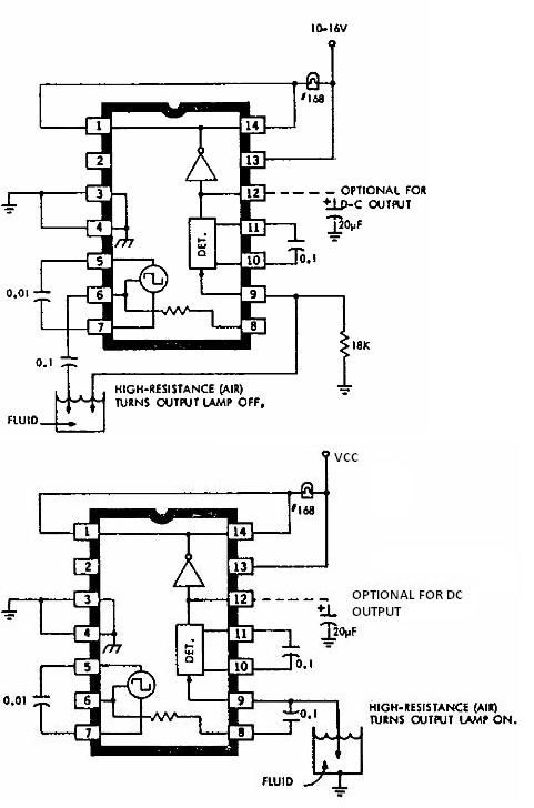
This electronic liquid detector circuit diagram is based on the ULN2429 monolithic bipolar integrated circuit designed for detecting the absence or presence of many different types of liquids. The ULN2429 electronic liquid detector circuit can be used in automotive,...
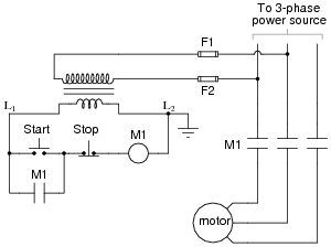
The most challenging aspect of interpreting ladder diagrams, particularly for individuals familiar with electronic schematic diagrams, is the representation of electromechanical relays. The operation of a motor control circuit should be explained, detailing what occurs when the "Run" switch...
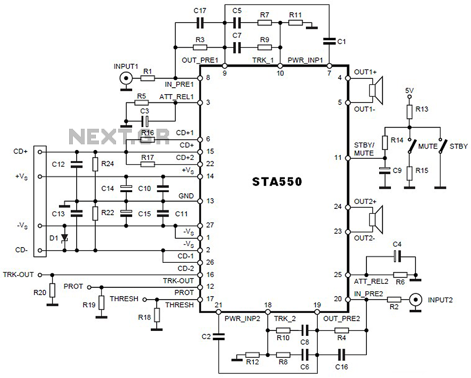
This is a 2 x 70W audio power amplifier circuit built using a single IC STA550. The amplifier circuit requires a few external components, primarily resistors and capacitors, and is straightforward to design. The STA550 audio amplifier can provide...

A CMOS-based circuit designed for adjusting the time of spot welding. This circuit utilizes a CMOS device that allows for cycle selection ranging from 1 to 99 cycles. In practical applications, most users find that adjustments within 10 cycles...