
Mark 2 Memory circuit

The memory architecture of the Mark 2 system is designed for efficiency and flexibility. The dual 32K FRAM chips enable a compact memory solution while allowing for quick access and manipulation of data. The use of the MREQ signal in conjunction with the A15 address line to select between the two chips optimizes the memory mapping, making it straightforward for the Z80 processor to interact with the memory. The design choice to forgo a ROM chip in favor of utilizing RAM for boot code storage provides a significant advantage in terms of resource utilization. This approach allows for dynamic memory allocation and eliminates the limitations commonly associated with fixed ROM storage.
The logic design implemented to generate the chip select signals exemplifies a practical application of digital logic principles. By using NAND and NOT gates, the circuit achieves the necessary functionality without the need for additional OR gates, thus simplifying the overall design. The implementation of De Morgan's Laws in this context showcases the versatility of digital logic, enabling the designer to adapt available components to meet specific requirements.
The consideration of using pull-up resistors with the FRAM chips highlights the importance of robust circuit design, particularly in ensuring data integrity during power transitions. The recommendation to use a 10K or 4.7K resistor demonstrates a proactive approach to mitigating potential issues that could arise from power fluctuations. This attention to detail can significantly enhance the reliability of the memory system, making it suitable for various applications where data retention during power cycles is critical. Overall, the memory architecture of the Mark 2 system is a well-thought-out design that balances simplicity, functionality, and reliability.The memory part of my Mark 2 system is extremely simple. There are two 32K SRAM chips (actually FRAM because I had them lying around, but there isn`t any significant difference in this application). These are selected with the logical OR of the MREQ signal and A15 (or inverse of A15 for the upper chip).
Because the boot code for the Z80 is held by the PIC and the PIC can control the whole address bus while it holds the Z80 in reset the boot code is written to normal RAM after power-on. This provides the advantage of less decode logic, and no ROM chip, as well as allowing the whole of the memory space to be used by whatever application is running as there are no "unwriteable" regions.
The actual logic I used to generate the select signals is not OR gates, as there were none of these on the board, but NAND and NOT gates as I had spare of these from various other functions. The translation is based on De Morgan`s Laws about equivalence of inverted operators. Basically if I invert both inputs and output of an and gate it becomes an or gate. However since I have a NAND gate the output is already inverted, so inverting the inputs will make the output equivalent to my OR gate truth table.
This actually only requires one extra gate as I would have to invert A15 anyway, the inverted version is just used in the select for the other chip now, and the extra gate is a NOT gate on the MREQ signal. I`ve mentioned here that I`m using FRAM chips. I currently don`t plan to use them for storage of data however, as I have found them somewhat "temperamental" in home made circuits in the past.
If you are interested in storing data in them through power-cycles, it`s worth noting that somewhere in the data sheet it suggests using a pull-up resistor on the chip select pin, this avoids any glitches during power-on that could destroy data in the memory. I`ve used a 10K, or possibly even a 4K7 in the past, and noticed much improved resilience, so even if you don`t think your system should be doing anything while power isn`t fully on or off, it`s worth adding that pull up.
🔗 External reference
Related Circuits

The circuit illustrated by the PGA204/205 pertains to the shield drive circuit shown in the figure. It is demonstrated through interference theory and practical application that the cable shield, when transmitting weak signals, maintains a certain potential. This configuration...
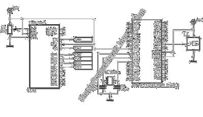
The LM35 from National Semiconductor is a precision centigrade temperature sensor that provides an analog output voltage. It operates within a temperature range of -55°C to +150°C and has an accuracy of ±0.5°C. The output voltage corresponds to 10mV...
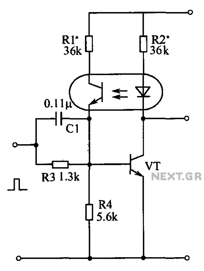
The bistable circuit and optocoupler transistor operate as illustrated in the accompanying figure. Initially, when the supply voltage is applied, the transistor VT is in the off state, resulting in a high output potential. Upon receiving a forward pulse...

The following circuit illustrates a 3V power supply designed for an RF remote control circuit. This circuit is based on the AT90S2323 integrated circuit (IC). Features include a data rate of 2400 bps. The 3V power supply circuit for the...

A dual-tone model train horn/sound generator/simulator circuit can be created using two NE 555 timers connected in cascade. However, the circuit diagram presented is designed with the NE 556 integrated circuit, which essentially comprises two 555 timers in a...
This low-power video transmitter is designed for remote control (R/C) applications, surveillance, or amateur radio purposes. It utilizes seven transistors within a crystal oscillator-multiplier RF power amplifier chain, along with a high-level video modulator. A supply voltage of 9...