
MAX4685 circuit and input current limit resistors

The MAX4685 is a low-voltage, dual analog switch designed for low on-resistance and high-speed switching applications. In a typical configuration, the device can be used to connect either of the two inputs, VI1 or VI2, to a common output.
For the connection diagram, it is essential to identify the pins of the MAX4685. The device features a total of 8 pins, with the following key pin functions:
1. **V+ (Pin 1)**: This pin is connected to the positive supply voltage, typically ranging from 2.7V to 12V.
2. **GND (Pin 4)**: This pin is connected to the ground of the circuit.
3. **IN1 (Pin 2)**: This pin is the control input for switch S1, determining whether VI1 is connected to the output.
4. **IN2 (Pin 3)**: This pin is the control input for switch S2, determining whether VI2 is connected to the output.
5. **COM (Pin 5)**: This is the common output pin where the selected input (either VI1 or VI2) will be directed.
6. **NO (Pin 6)**: This pin connects to the normally open terminal of switch S1.
7. **NC (Pin 7)**: This pin connects to the normally closed terminal of switch S1.
8. **GND (Pin 8)**: This serves as an additional ground reference.
To implement the switching functionality, the control inputs IN1 and IN2 should be driven high or low, depending on the desired connection. When IN1 is high, VI1 is connected to COM, while IN2 being high connects VI2 to COM. It is crucial to ensure that both control inputs are not activated simultaneously to avoid short-circuiting the supply.
The circuit design should also include bypass capacitors close to the V+ and GND pins to filter out noise and ensure stable operation. Additionally, proper consideration must be given to the load connected to the COM pin, as excessive current may exceed the switch's ratings, leading to potential damage.
In summary, the MAX4685 analog switch can effectively manage the connection between two input signals and a common output, allowing for versatile signal routing in various electronic applications. Proper attention to the control logic and electrical characteristics will ensure reliable performance in the intended application.Dear friends i need your advice about the connection diagram of the MAX4685 analog switch attached. I have two inputs VI1 and VI2 and hence we have.. 🔗 External reference
Related Circuits
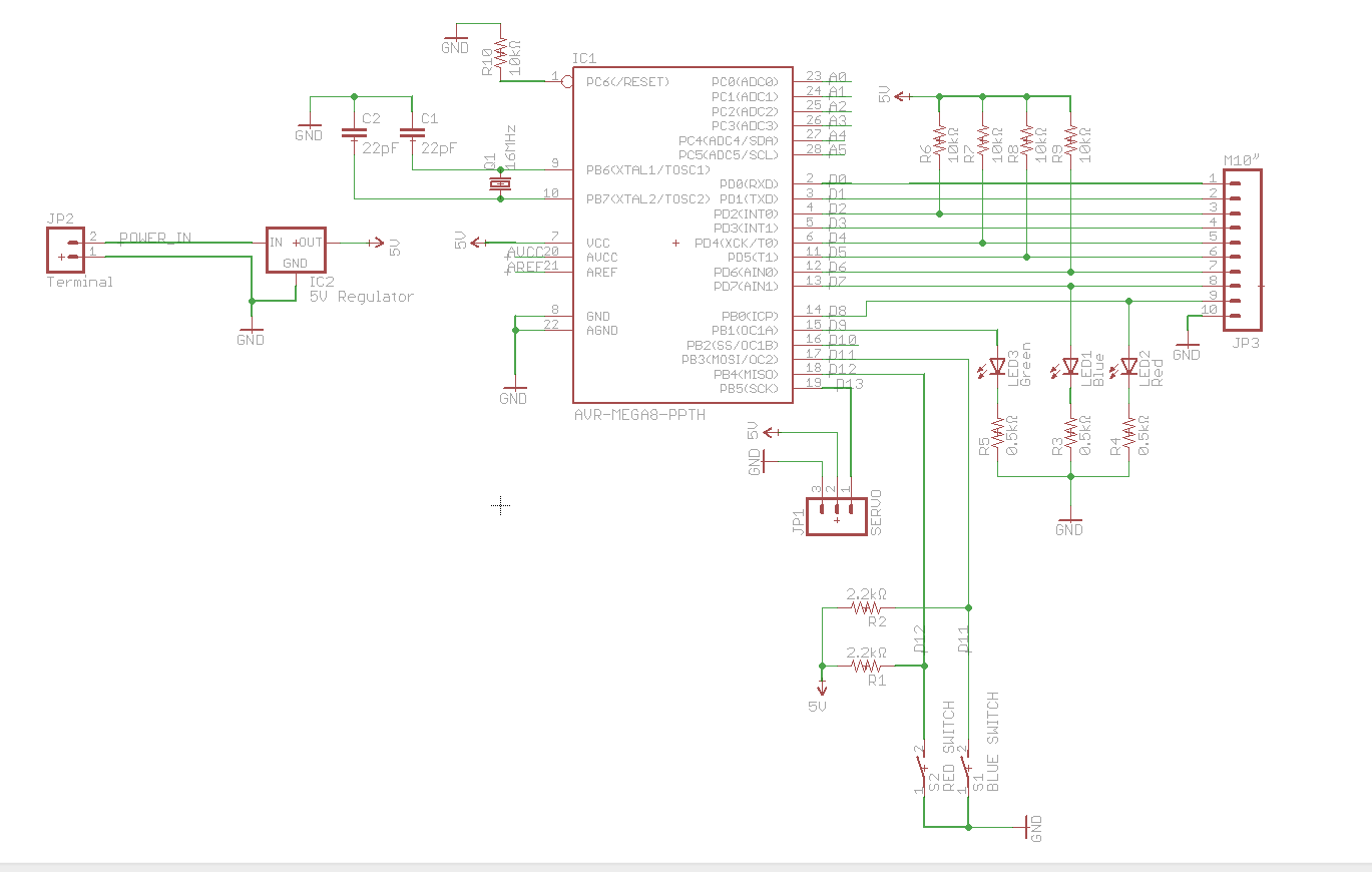
A circuit utilizes a keypad, a servo, and several LEDs, connected to an Arduino Uno. The objective was to integrate all components onto a single PCB, effectively creating a custom version of the Arduino. Upon startup, the red LED...

The circuit utilizes an integrated amplifier, resulting in a simple and compact design. The TDA4050 IC is employed, where a weak signal is received by the infrared photodiode (VD) and first passes through a transistor amplifier. The circuit is...

The founts must notify the server when the cup is taken from the fount or when the opponent's cup is poured into the team's cup. The implementation of the actual pouring action is at the discretion of the team....
The automatic emergency light circuit has the following features: 1. When the mains supply (230V AC) is available, it charges a 12V battery up to 13.5V, after which the battery is disconnected from the charging section. 2. When the...
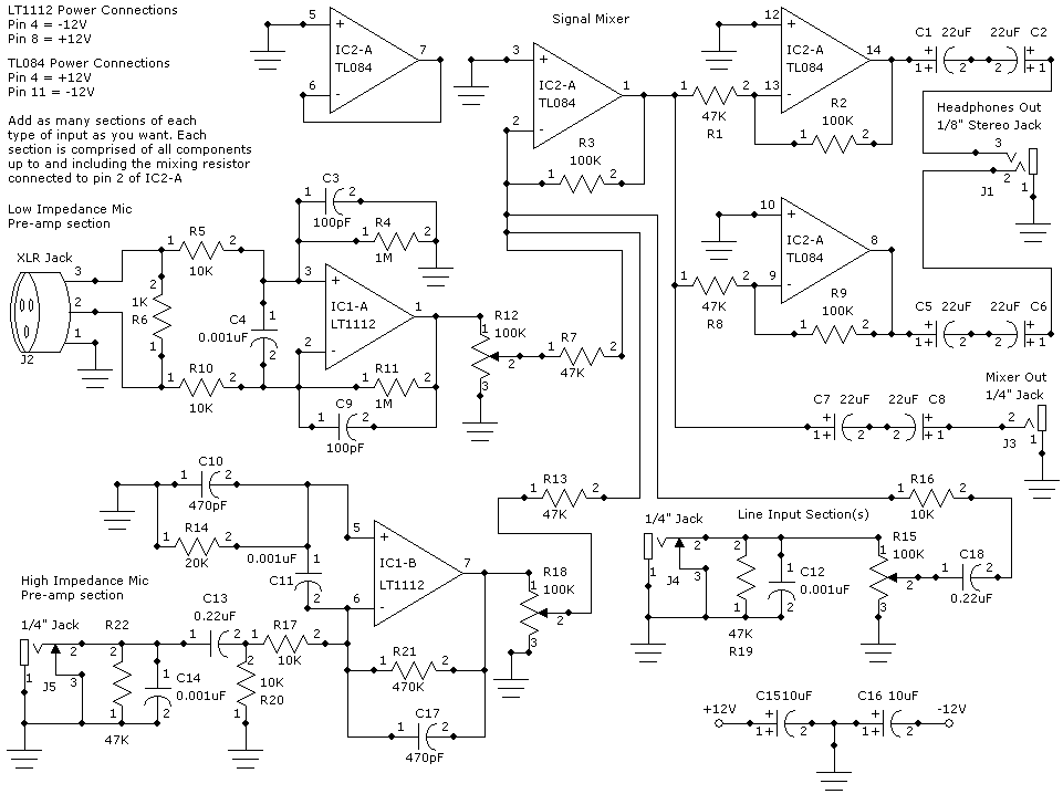
This weblog focuses on electronic circuit schematics, PCB design, DIY kits, and diagrams for various electronic projects. It features a mixer that demonstrates how to create microphone pre-amplifiers suitable for both low and high impedance microphones. The design utilizes...
The circuit operates correctly on a breadboard, with the LED blinking at a frequency of 2 Hz. However, when soldered onto a perfboard, the LED blinks at a significantly higher frequency, approximately 10 Hz, although this is an estimation...