
Maytag Neptune Schematic

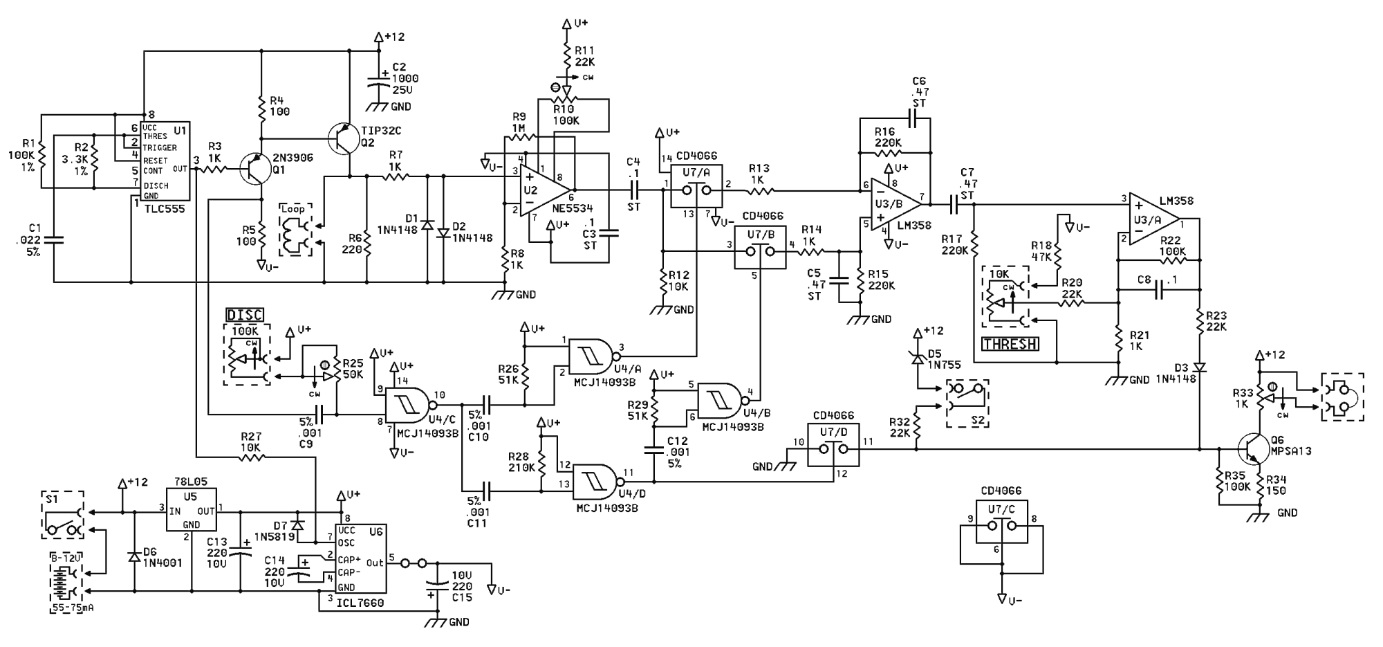
The motor control circuit described operates in a three-phase configuration, where each phase is controlled by a dedicated MOSFET to drive the motor effectively. The use of the IR2101 high-low driver IC allows for efficient control of the MOSFET gates, enabling rapid switching and improved performance of the motor drive. The failure of the Q5 MOSFET indicates a potential overcurrent condition, likely exacerbated by insufficient surge suppression, as indicated by the subsequent damage to diode D9.
In the design, the 75-ohm resistor J12 plays a critical role in limiting the gate current to the MOSFET, ensuring that the MOSFET operates within its safe limits. The addition of inline fuses between the motor harness and the control board serves as a protective measure, safeguarding the circuit from future overcurrent events. The presence of Zener diode Z1 is crucial for voltage regulation and protection against voltage spikes that could damage sensitive components in the circuit.
The layout of the circuit components, including resistors R1, R3, R10, and R12, and capacitor C39, is designed to minimize noise and interference, which can adversely affect the operation of the motor control system. Proper thermal management of the MOSFETs and diodes is essential, as overheating can lead to premature failure. The overall design emphasizes reliability, particularly in applications where the motor is subjected to varying loads, necessitating robust surge protection and effective thermal dissipation strategies.This circuit is basically repeated for each of the 3 motor phases. Here is my experience with repairing the motor control board in this washer. The Q5 mosfet blew out on c phase of the motor drive circuit and the 75 ohm resistor labeled J12 driving this mosfet was fried. The repaired washer operated properly until the 7th run which had a larger load than any of the previous
runs and then c phase blew out again and this time the damage extended to the zener diode Z1. After this blowout I focused more on checking the motor windings for problems, and tried to find any evidence of the motor wiring harness insulation being pinched or worn thru. Since the blowout occurred during a much heavier load than the previous runs and I couldn`t find any motor or motor wiring problems.
I concluded that the Q5 mosfet blowout might have been caused by the breakdown of surge suppression diode D9. This time I replaced diodes D9 & D11, mosfets Q5 & Q6, gate resistor labeled J12, IR2101 high low driver IC3, and the 15 volt zener diode Z1 and added inline fuses between the c phase motor harness wires and the control board.
View of board corresponding to the top right section of the schematic below. R1 & R3 are in the center, C39 is above Z1, and R10 & R12 are in the top right corner of the picture. 🔗 External reference
Related Circuits
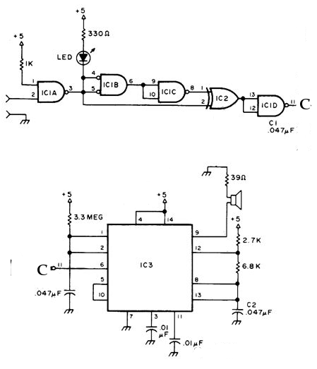
The NE556 timer can function as an indicator for the static state of a digital logic audible terminal. An audible logic probe is beneficial for visually inspecting a component while simultaneously checking the logic state at another point far...

Electronic FM Telephone Transmitter Schematic. The following schematic design illustrates a circuit diagram for an FM telephone transmitter built on a compact PC board layout. This small design allows it to be easily integrated within the housing of a...
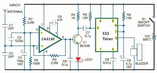
This electronic schematic allows for the design of a simple cellular phone detector circuit capable of sensing the presence of an activated mobile phone from a distance of 1.5 meters. The capacitor C3 should have lead lengths of 18...
If the TIP32C (Q2) transistor becomes excessively hot, consider replacing it with an IRF9640 MOSFET. It is advisable to experiment with different resistor values for R6 to determine the optimal resistance (a 390-ohm resistor is recommended). A trim potentiometer...
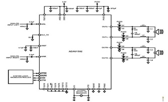
This is a typical stereo application circuit schematic of the ADAU1592, a 2-channel, bridge-tied load (BTL) switching audio power amplifier. The ADAU1592 can be utilized in flat panel televisions, PC audio systems, and mini-component applications. The ADAU1592 is designed to...
This circuit is designed for children's entertainment and can be installed on bicycles, battery-powered cars, motorcycles, as well as models and various games and toys. When switch SW1 is positioned as indicated in the circuit diagram, it generates the...