
Micropower double ended limit detector

The circuit employs four 1 megohm resistors, R1, R2, R3, and R4, which serve to convert the bipolar ±10V swing of the operational amplifiers to a 0 to 5V swing that is compatible with ground-referenced CMOS logic.
The primary function of this voltage monitor is to provide a reliable indication of whether the input voltage is within the predefined thresholds. The L144 sections act as voltage comparators, monitoring the input voltage against the set limits, Vhigh and Vlow. When Vin exceeds Vhigh, or falls below Vlow, the output of the NAND gate transitions to a logical high state, signaling that the monitored voltage is outside the acceptable range. Conversely, when Vin is within the specified limits, the output remains low.
The choice of using a CMOS NAND gate is significant due to its low power consumption characteristics, making it suitable for battery-operated devices or applications where power efficiency is critical. The resistors R1 through R4 play a crucial role in ensuring that the analog signals from the operational amplifiers are scaled down appropriately to avoid damage to the CMOS logic and to ensure accurate logical interpretation.
In summary, this voltage monitor circuit effectively combines the functionality of operational amplifiers and CMOS logic to provide a robust solution for monitoring voltage levels in various electronic applications, ensuring that the output accurately reflects the input voltage conditions.The detector uses three sections of an L144 and a DC4011 type CMOS NAND gate to make a very low power voltage monitor. If the input voltage, Vin, is above Vhigh or below Vlow, the output will be a logical high. If (and only if) the input is between the limits will the output be low
The 1 megohm resistors Rl, R2, R3, and R4 translate the bipolar ±10V swing of the op amps to a 0 to LOV swing acceptable to the ground-referenced CMOS logic.
Related Circuits
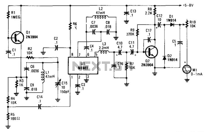
In this circuit, oscillator Q1 operates at approximately 15 kHz and provides input to mixer U1. U1 contains an internal oscillator that also runs at around 15 kHz. Capacitor C15 is employed to achieve zero-beat between both oscillators. When...
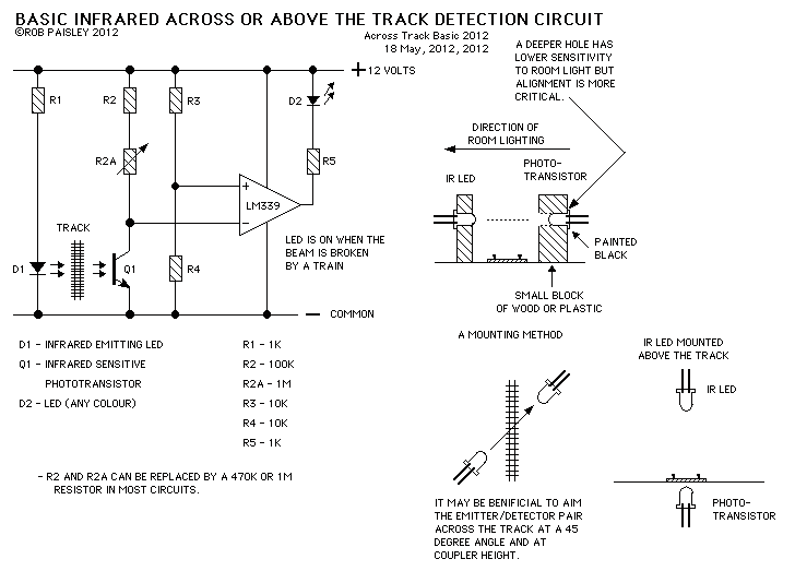
This page presents information on infrared - Across The Track train detection circuits. The circuits are designed around the LM339 comparator chip and can use a wide assortment of matched infrared - emitter / detector pairs. The basic circuit...
The ICM7226 is a fully integrated Universal Counter and LED Display driver. It combines a high-frequency oscillator, a decade timebase counter, an 8-decade data counter and latches, a 7-segment decoder, digit multiplexer, and segment and digit drivers, which can...
The oscillator is a standard UHF design that delivers approximately 10 mW at a frequency of 1.2 GHz. Resistors R1 and R2 bias the base of transistor Q1 to 1.2 V through a 12-ohm resistor. The collector current is...

The circuit employs negative feedback exclusively for positive signals. The inverting input receives feedback only when diode D1 is forward biased, which occurs solely with positive input signals. As the positive input signal increases, the output of the operational...
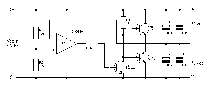
Another circuit for a balanced diet from a single voltage network. In fact, this is a uitbreding the other voltage divider circuit using a some power darling tons as buffer. This buffer can deliver a 200 to 300 mA....