
Monitor circuit diagram with over 555

The 555 timer IC is a highly versatile component widely used in various electronic applications due to its ability to operate in different modes. The configuration of the circuit is dependent on the connections made to the external components, including resistors, capacitors, and switches. The K1 and K2 switches play a crucial role in determining the operational mode of the circuit.
In the first mode, when K1 and K2 are both set to position one, the circuit functions as a precise exposure timer. This mode allows for timing adjustments from 0 to 100 seconds, making it suitable for applications such as photography where specific exposure durations are required. The timing is controlled by the RC network formed by the resistors and capacitors connected to the timer.
In the second mode, with K1 and K2 in position two, the circuit's output at pin 3 is disconnected, which effectively isolates the dimming circuit. This allows for independent control of the light intensity by adjusting the variable resistor RP2. The configuration enables the user to determine the necessary exposure time for film by measuring the output voltage corresponding to the light intensity.
The third mode, activated by setting K1 to position three and K2 to position one, transforms the circuit into a light control switch. This configuration utilizes the variable resistor RP2 and transistor VT2 to adjust the trigger point of the timer IC, providing flexibility in light control applications.
Finally, in the fourth mode, the functionality of the delay can be toggled based on the position of switch K2. This allows for the implementation of a delayed activation feature, which can be useful in various timing applications where a specific delay is required before the circuit becomes active.
Overall, this circuit exemplifies the flexibility of the 555 timer IC, demonstrating its capability to function as a timer, dimmer, light control switch, and delay circuit through simple adjustments of external components and switches.Depending on the external circuit connection, 555 may be formed start delay, trigger delay, multi-harmonic oscillation mode and other working conditions, it is with some RC com ponents, switches and the like multi-purpose tester. By setting the control of the K1, K2 switch, the circuit can have exposure timing, dimming, delay and other functions. When the K1, K2 set to 1 position, it can be used as 0 to 100 second exposure timing circuit. When the K1, K2 are placed in the 2 position, IC 3 feet dimming circuit is broken K1-4, VT4 was K2-2 short front and rear circuit is independent state.
In this state, adjust the scale value on RP2, can be measured to know the exposure time required for the film. When K1 is set to 3 position, K2 is set to 1 for light control switch circuit, RP2 VT2 for adjusting the trigger end of the IC from the control point.
When K1 is set to 4, you need to select the location of the delay based on K2, the delay can be opened and closed function is activated.
Related Circuits
This document describes an electronic winding machine with manual, electric, and semi-automatic features. The specific example highlighted includes an electronic counting function that assists users in managing motor windings. The circuit design consists of various components as illustrated in...
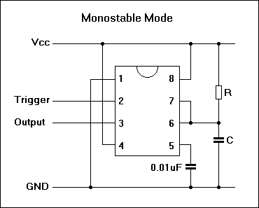
In the 555 datasheet, there is a pulse width modulation circuit that resembles this one, with the only difference being that pin 5 is labeled as 'audio'. The 555 timer IC is a versatile device commonly used in various applications,...

The schematic diagram of a 100W inverter circuit converts a 12V DC input into a 220V AC output. The circuit is built using the IC CD4047 to generate a 50Hz sine wave signal. The power transistor 2N3055 amplifies the...

A very simple FM IF MW radio receiver circuit can be designed using the LA1260 IC manufactured by Sanyo Semiconductor. This FM IF MW radio receiver circuit schematic shows that the LA1260 IC can be utilized in AM and...
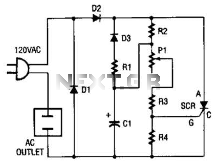
This circuit allows any standard household bulb to shimmer or blink. It is compatible with incandescent lights up to 200 W and operates on standard 120 Vac. The circuit employs a silicon-controlled rectifier (SCR) to create the shimmering effect....
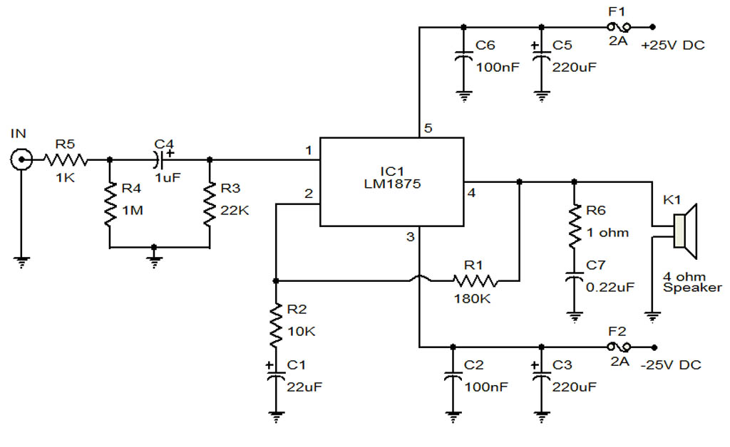
The circuit illustrates a 20-Watt audio amplifier diagram based on the LM1875 integrated circuit (IC). It is designed for use in automotive applications and provides an output power of 20 Watts. The 20-Watt audio amplifier circuit utilizing the LM1875 IC...