
multi output dc to dc converter lm2596

The LM2596-based DC to DC converter circuit is designed to efficiently convert a varying input voltage within the specified range into multiple regulated output voltages, making it suitable for various electronic applications. The LM2596 is a step-down (buck) voltage regulator that is widely recognized for its reliability and efficiency in power conversion.
The circuit configuration typically includes an inductor, a diode, and capacitors, which work together to stabilize the output voltage. The inductor stores energy when the switch (usually a transistor) is closed and releases it when the switch opens, maintaining a steady output voltage. The feedback mechanism ensures that the output voltage remains constant, despite variations in the input voltage or load current.
In practical implementations, the circuit may include additional components such as input and output capacitors for stability and filtering. The input capacitors help to smooth out the input voltage, while the output capacitors reduce voltage ripple and improve transient response. The choice of inductor and diode is critical, as they affect the overall efficiency and performance of the converter.
The application of this converter is particularly beneficial in systems requiring multiple voltage levels from a single power source, such as embedded systems, communication devices, and audio equipment. The regulation accuracy of ±5% for the lower voltage outputs ensures that sensitive digital logic circuits receive stable power, while the ±20% regulation for the higher voltage outputs is often sufficient for analog applications like operational amplifiers.
Overall, this LM2596-based DC to DC converter circuit is an effective solution for providing multiple regulated outputs from a single input supply, with a balance of efficiency, regulation accuracy, and low ripple voltage, making it suitable for a wide range of electronic applications.This is the circuit diagram of DC to DC converter based LM2596, the circuit has a single input supply and multiple voltage outputs. The circuit has an input voltage range of 15V to 40V. It has 5 outputs: 3. 3V at 1. 5A; +12V and ’12V at 50 mA each; and +5V and ’5V at 50 mA each. The 3. 3V, +5V and ’5V outputs are regulated with ±5% accuracy o ver line and load variations. The +12V and ’12V outputs are regulated with ±20% accuracy. A typical application of this circuit is where the 3. 3V output provides the power to the main circuit which is 3. 3V logic, the ±5V outputs power the 5V logic and ±12V outputs provide the bias supply of op-amps. The efficiency of the circuit with full load at all outputs is 75%. The ripple voltage across the 3. 3V output is less than 20 mV and that across the ±12V outputs is less than 30 mV. The ripple across the ±5V is less than 10 mV. 🔗 External reference
Related Circuits
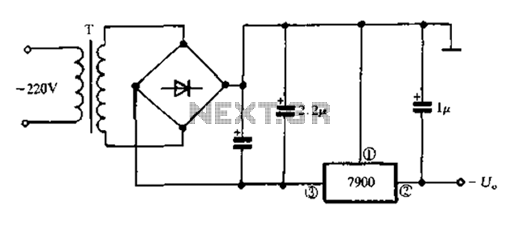
7900 series three-terminal fixed negative output voltage regulator circuit The 7900 series comprises a range of three-terminal fixed negative voltage regulators designed to provide stable output voltages. These regulators are specifically engineered to deliver a consistent output voltage, which is...
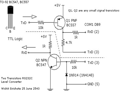
To connect a microcontroller project to the COM port of a PC, an RS-232 converter is required. Various chips are available to address this need, such as the MAX232 and DS275. The RS-232 standard is widely used for serial communication...
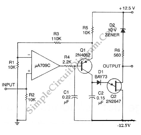
The voltage to frequency converter (V/FC - VCO) circuit consists of a UJT (uni-junction transistor) oscillator in which the timing charge capacitor C2 is utilized. The voltage to frequency converter circuit operates by converting an input voltage into an output...
Significant overengineering was necessary to replicate a previous capacitive scanner. At the local hackerspace OSAA, a brainstorming session was initiated with Pedersen, AsbjG rn, and Flemming, who quickly generated numerous creative ideas. The discussion took an interesting turn when...
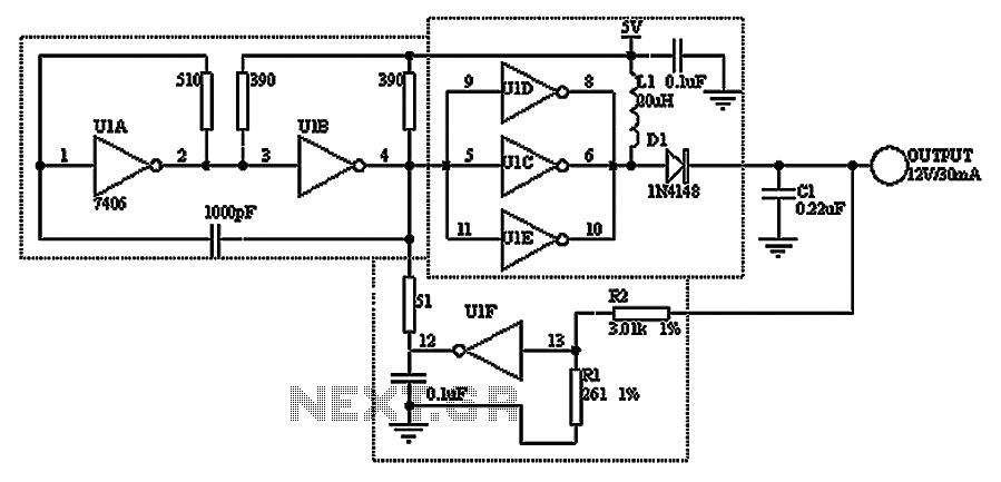
A TTL hex inverter circuit can function as a DC/DC converter, converting 5V to 12V. This circuit encompasses all necessary functionalities for DC/DC conversion. It relies on a TTL switching threshold voltage regulator. The components U1A and U1B form...
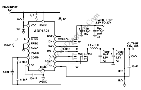
This is an ADP1821 step-down DC-to-DC converter circuit. This circuit utilizes the ADP1821, which is a synchronous pulse-width-modulated (PWM) step-down controller. The ADP1821 is designed to efficiently convert a higher input voltage to a lower output voltage while maintaining high...