
Multipurpose Flip-Flop Timer

The timing circuit is structured around a CMOS 4011 quad NAND gate, which is an integrated circuit featuring four two-input NAND gates. In this implementation, two of the gates are configured to function as a Set/Reset flip-flop, enabling the timing mechanism. The flip-flop's ability to maintain its state based on the input signal from switch S1 is crucial for initiating the timing sequence. The charging of capacitor Cx through potentiometer Rx is the primary method of timing, with the time delay being adjustable based on the selected resistor value.
The circuit's design ensures that during the timing period, both the relay and LED are activated to provide visual and functional feedback. The use of transistors Q1 and Q3 allows for effective control of the relay and LED, while also ensuring that the circuit can handle the required current without damaging the NAND gate. The reset mechanism, utilizing diode D1 and the capacitor, guarantees that the circuit is in a known state upon power-up, preventing unintended operation.
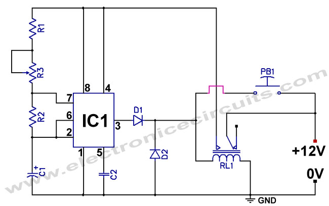
The choice of a 12V power supply is practical for many applications, and the inclusion of a voltage regulator ensures stable operation of the logic components. The protection diodes (D3 and D4) enhance the reliability of the circuit by preventing damage due to reverse polarity and inductive kickback from the relay. Overall, this timing circuit is versatile and can be adapted for various timing applications by simply adjusting the values of Cx and Rx, making it a valuable addition to any electronic project requiring time delay functionality.This particular timing circuit can be used to time one-shot events from a few seconds to a few hours. And in standby mode (ie, with RLY1 and LED1 off), its power consumption is very low. The heart of this circuit is a low-cost CMOS 4011 quad NAND gate, with IC1a & IC1b configured as a standard Set/Reset flip-flop.
Briefly pressing switch S1 to sta rt the timing sequence pulls pin 1 of IC1a low and, as a result, pin 3 switches high. Two things happen while pin 3 is high: capacitor Cx begins charging via potentiometer Rx; and (2) pin 11 of IC1d will be low, which means that transistors Q3 and Q1 are both on. As a result, both LED 1 and relay RLY1 are also on. RLY1 and LED 1 remain on until Cx has been charged up to about 70% of Vcc (ie, the supply rail). At this point, pins 8 & 9 of IC1c are pulled high and so its pin 10 output goes low and resets the flip-flop by applying a low to pin 6 of IC1b.
This causes pin 3 of IC1a to go low and so LED1 and RLY1 switch off and the timing period ends. At the same time, pin 4 of the flip-flop goes high and this turns on transistor Q2 while ever the flip-flop is held reset. This ensures that Cx is discharged, so that the circuit is ready the next time S1 is pressed. Diode D1 and its associated 10 µF capacitor reset the flip-flop when power is first applied, so that LED1 and RLY1 remain off until S1 is pressed.
D4 is included to protect Q1 against the back-EMF that`s generated when the relay switches off. Choosing appropriate values for Cx & Rx for a given time delay is straightforward. The formula is T = 1. 24 x Rx x Cx, where T is the delay time in seconds. As an example, let`s assume that we require a time delay of 10s using a value of 100 µF for Cx. Now we just need to calculate the value of Rx as follows: In this case, an 82kO resistor would be the closest value. You can use either a fixed resistor for Rx or you can use a potentiometer (or trimpot) which can be adjusted to give the required time delay.
Note that the value of Rx should not be any more than a few megohms. Power for the circuit can be derived from any 12V DC source. This is then fed to 3-terminal regulator REG1 to derive a 9V rail to power the circuitry. The exception here is the relay circuit, which is powered from the 12V rail. Diode D3 protects the circuit against incorrect supply polarity. 🔗 External reference
Related Circuits
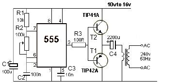
This 12V power inverter circuit can be utilized to power small devices that require 240 volts. It is particularly advantageous for operating 240-volt appliances using a 12-volt car battery. Unlike typical feedback oscillator inverters, this design employs a 555...
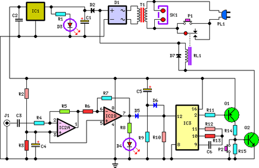
This circuit deactivates an amplifier or any connected device when a low-level audio signal at its input is absent for at least 15 minutes. Pressing P1 turns the device on, supplying power to any appliance connected to SK1. The...
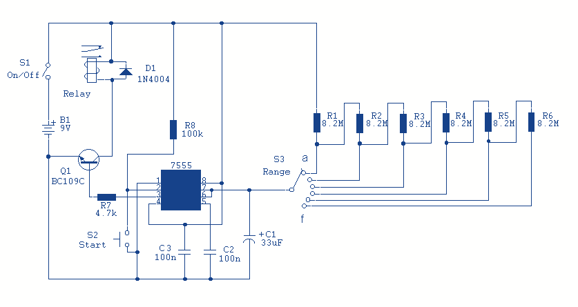
A switched timer for intervals of 5 to 30 minutes incremented in 5 minute steps. Simple to build, simple to make, nothing too complicated here. However, you must use the CMOS type 555 timer designated the 7555; a normal...
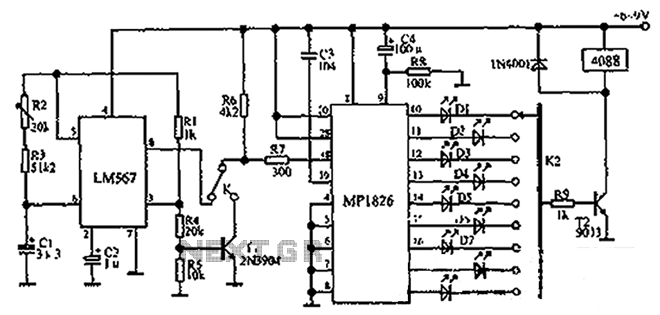
The circuit illustrated in the figure incorporates the MP1826 as a multi-stage divider. The LM567 serves as the frequency demodulation component, functioning as a dual-band oscillator that generates the desired low-frequency pulse from the MP1826. The oscillation center frequency...
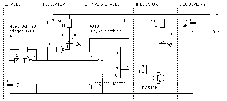
The CLOCK input indicates that it is edge-triggered, responding to abrupt changes in voltage rather than gradual changes or steady logic levels. The CLOCK input of the 4013 D-type bistable is specifically rising-edge triggered, meaning it only reacts to...
The standard 555 timer circuit consumes power from the battery even when the start push-button (PB1) is not pressed, due to a potential divider created by three 5kΩ resistors within the integrated circuit (IC). This power consumption, referred to...