
Musical Instrument Digital Interface (Midi) Receiver Circuit
 Receiver")
The circuit design incorporates the SFH250 photodiode, which is sensitive to light and is capable of detecting modulated optical signals. The photodiode's output is a small current proportional to the light intensity, which is then amplified for further processing. Buffer T2 serves a critical role in isolating the photodiode from the subsequent amplification stages, ensuring that the signal integrity is maintained while preventing loading effects.
The cascade amplifier, comprised of transistors T3 and T4, is configured to provide significant gain to the weak signals generated by the photodiode. This stage is essential for boosting the signal strength to a level suitable for the operational amplifier IC4, which is configured to further refine and amplify the signal. The operational amplifier may also incorporate filtering to remove any unwanted noise from the signal.
Following the operational amplifier, the buffered outputs from IC5-f and IC5-e are designed to drive subsequent stages or components, ensuring that the signal can be effectively utilized in downstream applications. The use of buffers helps maintain signal integrity and prevents any loading on the previous stages.
Power supply considerations are addressed by IC6, which provides a stable 9 V to the entire circuit. This voltage level is crucial for the proper operation of the amplifying components and ensures that the circuit functions reliably under varying load conditions. Overall, this schematic effectively converts optical data into usable electrical signals, ensuring high fidelity and performance in data transmission applications. Receiver photodiode SFH250 is used to convert optical data pulses at 32.5 Kb to electrical signals. Buffer T2 feeds the signals to cascade amplifier T3-T4, then to op amp IC4, and buffers IC5-f and IC5-e. IC6 supplies 9 V for the circuit.
Related Circuits

The subwoofer is a speaker designed to reproduce low frequencies, specifically in the range of 20 Hz to 150 Hz. The electronic circuit diagram below illustrates the details of a subwoofer amplifier using the TDA1516, a 22-watt amplifier suitable...
This circuit is designed to maintain the liquid level between two fixed points. By transforming the K1 contacts off the case, it can perform filling or extraction operations in two modes. The load can be either an AC motor...

Proper grounding is essential for eliminating hum and ground loops. Connect the ground terminals of J1, P1, C2, C3, and C4 to the same point. Connect C6 to the output ground. An audio amplifier is an electronic device that...
This caller ID circuit utilizes the Motorola MG145447 IC chip. The service must be available from your local phone company for this circuit to function properly. The caller ID circuit based on the Motorola MG145447 IC chip is designed to...
One of the critical components is a PWM speed controller, allowing for fine speed adjustments instead of just an "on" mode that runs at full power. This is important for safety. A basic stamp microcontroller was purchased, which includes...
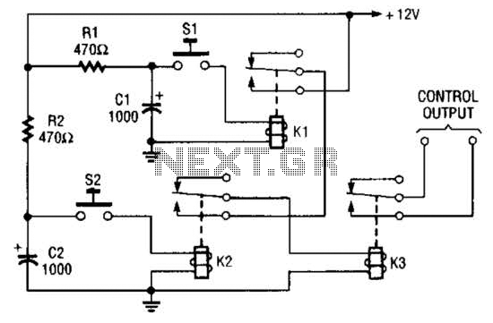
Due to the limited hold-on time of the delay circuits R1/C1 and R2/C2, both switches S1 and S2 must be activated simultaneously to energize the load. The circuit in question involves a delay mechanism governed by the time constants associated...